Abstract
A research team led by Professor Joonki Suh in the Graduate School of Semiconductor Materials and Devices Engineering and the Department of Materials Science and Engineering at UNIST, in collaboration with Professor Feng Ding from the Chinese Academy of Sciences in China, Professor Sungkyu Kim from Sejong University, and Professor Changwook Jeong of UNIST, has developed a revolutionary thin film deposition process for tin selenide-based materials. This process utilizes the metal-organic chemical vapor deposition (MOCVD) method, enabling thin film deposition on large wafer surfaces at a low temperature of 200°C, achieving exceptional precision and scalability.
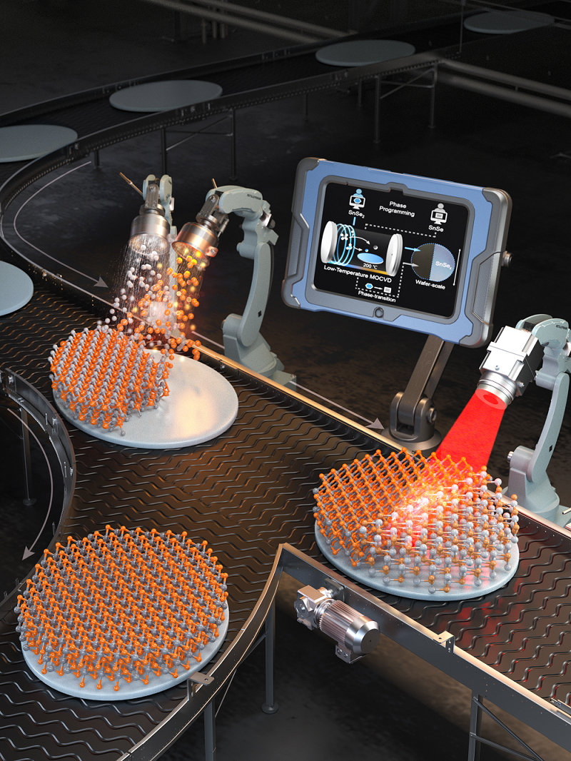
Figure 1. A cover image, proposed for the April 2024 issue of Advanced Materials.
MOCVD is a cutting-edge technique that employs gaseous precursors to carry out chemical reactions with outstanding precision, making it possible to deposit thin films on wafer-scale materials used in semiconductors. Thanks to this innovative method, the team was able to synthesize tin selenide materials (SnSe2, SnSe) with uniform thicknesses in just a few nanometers on wafer units.
To achieve deposition at low temperatures, the team strategically separated the temperature sections for ligand decomposition and thin film deposition. By adjusting the ratio of tin and selenium precursors as well as the flow rate of argon gas carrying the precursor, they were able to meticulously control the deposition process, resulting in high crystallinity, regular alignment, and controlled phase and thickness of the thin films.
This advanced process allowed for the uniform deposition of thin films at a low temperature of approximately 200°C, regardless of the substrate used, showcasing its potential for various electronic applications on a large scale. The team successfully applied this method to the entire wafer, maintaining chemical stability and high crystallinity in both types of tin selenide thin films.
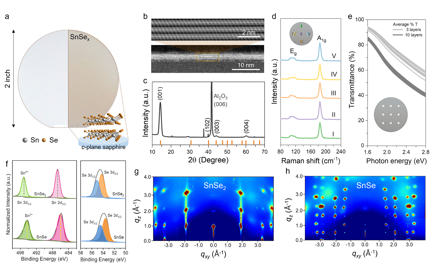
Figure 2. (a) Schematic image, showing the direct MOCVD growth of wafer-scale 2D SnSe2 films. (b) Cross-sectional HAADF-STEM images of SnSe2 ultra-thin films along a (100) zone axis. c) XRD pattern of as-grown 3L-SnSe2 films on a c-axis sapphire substrate. (c) Raman scattering spectra of 3L-SnSe2 films taken at five representative locations marked on the wafer as illustrated in the inset. (f) The high-resolution XPS demonstrated the valence states and chemical composition of the film after the phase transition. (g, h) The directly grown SnSe2 and the phase-transited SnSe film were characterized by synchrotron-based GI-WAXD.
Lead author Sungyeon Kim emphasized the significance of this study in overcoming limitations of existing deposition methods, demonstrating the capability to deposit polyphase materials over large areas without altering chemical composition. This breakthrough opens doors for applications in electronic devices and further research on tin selenide-based materials.
Professor Suh highlighted the innovative nature of this study in proposing a unique process strategy based on thermodynamic and dynamic behavior according to the phase of semiconductor thin film materials. The team aims to advance research on electronic device applications by developing customized processes for next-generation semiconductor materials.
The research findings were published online in Advanced Materials on April 10, 2024. It has been carried out with funding support from the Ministry of Science and ICT, the National Research Foundation (NRF) of Korea, the next-generation intelligent semiconductor technology development project, and UNIST.
Journal Reference
Sungyeon Kim, Wookhee Lee, Kyungmin Ko, et al., "Phase-Centric MOCVD Enabled Synthetic Approaches for Wafer-Scale 2D Tin Selenides," Adv. Mater., (2024).


