UTokyo researchers have created an electronic component that demonstrates functions and abilities important to future generations of computational logic and memory devices. It is between one and two orders of magnitude more power efficient than previous attempts to create a component with the same kind of behavior. This fact could help it realize developments in the emerging field of spintronics.
If you're a keen technophile and like to keep up to date with current and future developments in the field of computing, you might have come across the emerging field of spintronic devices. In a nutshell, spintronics explores the possibility of high-performance, low-power components for logic and memory. It's based around the idea of encoding information into the spin — a property related to angular momentum — of an electron, rather than by using packets of electrons to represent logical bits, 1s and 0s.
One of the keys to unlock the potential of spintronics lies in the ability to quickly and efficiently magnetize materials. University of Tokyo Professor Masaaki Tanaka and colleagues have made an important breakthrough in this area. The team has created a component — a thin film of ferromagnetic material — the magnetization of which can be fully reversed with the application of very small current densities. These are between one and two orders of magnitude smaller than current densities required by previous techniques, so this device is far more efficient.
"We are trying to solve the problem of the large power consumption required for magnetization reversal in magnetic memory devices," said Tanaka. "Our ferromagnetic semiconductor material — gallium manganese arsenide (GaMnAs) — is ideal for this task as it is a high-quality single crystal. Less ordered films have an undesirable tendency to flip electron spins. This is akin to resistance in electronic materials and it's the kind of inefficiency we try to reduce."
The GaMnAs film the team used for their experiment is special in another way too. It is especially thin thanks to a fabrication process known as molecular beam epitaxy. With this method devices can be constructed more simply than other analogous experiments which try and use multiple layers rather than single-layer thin films.
"We did not expect that the magnetization can be reversed in this material with such a low current density; we were very surprised when we found this phenomenon," concludes Tanaka. "Our study will promote research of material development for more efficient magnetization reversal. And this in turn will help researchers realize promising developments in spintronics."
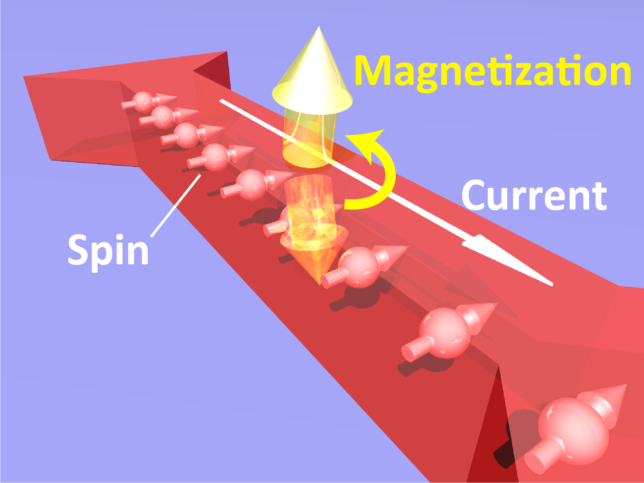
This diagram shows how magnetization reverses in a GaMnAs crystal. Image: © 2019 Tanaka-Ohya Laboratory


