Stacked layers of graphene can act like a mirror for beams of electrons. Physicists Daniël Geelen and colleagues discovered this using a new type of electron microscope. In an article in Physical Review Letters, they describe their results, which could lead to the development of optics for electron beams instead of light.
Geelen and co-workers dubbed the new technique 'eV-TEM'. It's a new variation of the electron microscope, which aims beams of electrons at a sample in order to image it.
Low energy electrons
According to quantum mechanics, electrons are waves, just as visible light is, but the wavelength is much shorter. Because of this, much smaller details can be imaged in comparison to a light microscope. However, the onslaught of electrons generally damages the sample in the long run.
This is one of the reasons that Daniël Geelen, Johannes Jobst, Sense Jan van der Molen and Rudolf Tromp use slow electrons, carrying low energies of several electron volts (eV, hence 'eV-TEM') instead of the usual tens or hundreds of thousands of electron volts.
Electrons in graphene
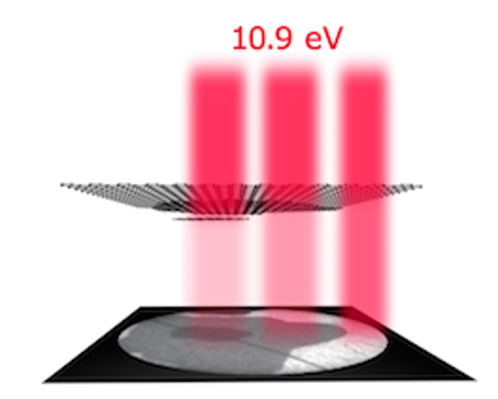
Since 2010, the group runs a LEEM (Low Energy Electron Microscope) developed by Tromp at IBM, which images the reflected electrons. Geelen enhanced the apparatus with a possibility to image the electrons that go through the sample, the 'transmission'. This turns the apparatus in a Transmission Electron Microscope (eV-TEM).
The first material investigated is graphene, the variety of carbon in a flat, two dimensional hexagonal molecular pattern resembling chicken wire. The researchers fired slow electrons at single, double and triple layers of graphene, and imaged the transmission.
'There has been much research into how electrons behave within graphene layers, but much less into how they move across layers,' says Sense Jan van der Molen.
Testing the theory
One theoretical model from the seventies predicts that slow electrons can pass through thin layers easily, as they will scarcely interact with the electrons within those layers. Then, when the energy and speed of the electrons is raised, the number of interactions is expected to increase, which would result in less and less electrons passing through the sample. This 'universal curve' is supposed to hold, regardless of the exact material of the sample.
The Leiden physicists however, noticed something very different. At specific electron energies, they measure sharp decreases in the transmission, which correspond to peaks in the reflection. 'For electrons with certain energies, the graphene acts as a mirror,' says Van der Molen.
Mirorring graphene
In the article, the researchers provide an explanation: electrons are waves. At certain wavelengths, the waves reflected off separate graphene layers will reinforce each other. This 'constructive interference' causes the stack of graphene layers to act as a mirror for electrons.
A similar effect is visible in the greenish or purplish hue of an antireflective coating on glasses or binoculars. They too consist of layers, which cause constructive interference for green or purple light.
The wavelength dependent mirroring proves that thin samples don't act so predictably and independently from the exact material as expected, says Johannes Jobst. 'These results depend strongly on the electron structure of the material, and on the electron energy.'
Additionally, the research suggests the possibility to use layered graphene as mirrors for electron beams. 'It may be possible to use them as beam splitters', says Tromp.
Thin layers less predictive
Such beam splitters, which split a single incoming beam into two separate beams, are much used standard devices in light optics, but they don't exist for electron beams yet. Thin layers of graphene could perhaps fill in this gap. But first, the researchers would like to image other materials. Van der Molen: 'This enables fundamentally new research, into layered materials, and also into sensitive biomolecules that would be damaged in a regular electron microscope.'
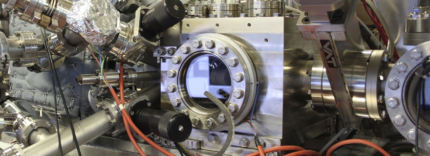
Top image: Low Energy Electron Microscope


