A semiconductor chip about the size of a thumbnail contains a maximum of billions of microelements, such as transistors and diodes. These microelements on the semiconductor chip are composed of fine patterns, and thus a lithographic process that uses electron beams is required for patterning.
An international team of researchers, affiliated with UNIST, has recently presented a novel technique for the fabrication of fine patterns without the need of a complex and costly process. Published in the February 2021 issue of ACS Nano, this breakthrough has been jointly led by Professor Seon Namgung (Department of Physics, UNIST) and researchers from the University of Minnesota, located in Minnesota of the United States.
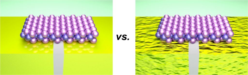
Figure 1. Schematic images showing a short-channel device built by transferring 2D materials on top of ultraflat template-stripped (left) and rough as-deposited (right) metal structures with nanoscale gap. In these device structures, the pair of metal bases work as electrodes connecting the transferred 2D material flake, while the nanogap between two elevtrodes functions as a channel for carrier transport. Since the electrical
In this study, the research team has developed a scalable method to build an ultraflat nanogap platform, which can be used for short-channel 2D material devices without directional restriction on device formation. In this approach, they also constructed two metal layers separated by a nanoscale gap as small as 10 nm, defined precisely by a sandwiched Al2O3 film deposited by an atomic layer deposition (ALD) process. The two metal layers with the nanogap separation are formed by a template-stripping method, resulting in metal layers with a root-mean-squared (RMS) roughness as low as 0.315 nm, smaller than the thickness of monolayer graphene. The two metal surfaces in the platform exhibited ultraflatness, and were vertically aligned without height difference, noted the research team.
"Since the electrical and optical properties of 2D materials are significantly affected by the roughness of the substrate, the ultraflat template-stripped Au used in our work should be advantageous compared to the rougher as-deposited Au platform for carrier transport in 2D materials with less contact resistance," noted the research team.
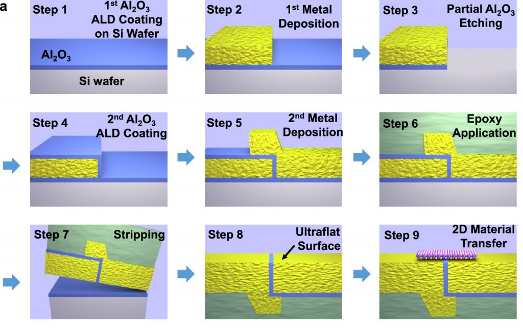
Figure 2. Fabrication of an ultraflat nanogap platform. (a) Schematic diagram showing the fabrication process of an ultraflat nanogap platform.
In this work, the research team demonstrated that the ultraflat platform can be used to build 2D material based short-channel field-effect transistors (FETs) and photodetectors. Simply by placing 2D material flakes on top of the platform, the research team fabricated short-channel FETs based on black phosphorus and MoS2 that exhibit their typical transistor characteristics. They also used the same platform to fabricate and demonstrate photodetectors with a nanoscale photosensitive channel, exhibiting higher photosensitivity compared to microscale gap channels. According to the research team, the two metal surfaces in the platform exhibited ultraflatness, and were vertically aligned without height difference.
"In this work, we demonstrated that the ultraflat platform can be used to build 2D material based short-channel FETs and photodetectors," says Professor Namgung, the first author of the study. "This simple approach, wherein 2D materials can be placed on top of predesigned ultraflat nanogaps, allows large-scale fabrication of 2D material-based short-channel devices."
He adds, "Our wafer-scale atomic layer lithography method can benefit a diverse range of 2D optical and electronic applications, including the development of miniaturized semiconductor structures, ultra-compact optical communication modules, as well as optical semiconductor chips."
The findings of this research have been published ahead-of-print in the online edition of ACS Nano on February 24, 2021. This study has been supported through the Basic Research Program in Science and Engineering by the National Research Foundation of Korea (NRF). This work has also been supported by the 2019 Research Fund of UNIST.
Journal Reference
Seon Namgung, Steven J. Koester, and Sang-Hyun Oh, "Ultraflat Sub-10 Nanometer Gap Electrodes for Two-Dimensional Optoelectronic Devices," ACS Nano, (2021).


