Femtosecond laser-induced periodic surface structures can be used to control thermal conductivity in thin film solids, report researchers from Japan. Their innovative method, which leverages high-speed laser ablation, produces parallel nanoscale grooves with unprecedented throughput that is 1,000 times stronger than conventional approaches, strategically altering phonon scattering in the material. This scalable and semiconductor-ready approach could make it possible to mass-produce thermal engineering structures while maintaining laboratory-level precision.
Using Lasers to Make Nanostructures That Control Heat Transport
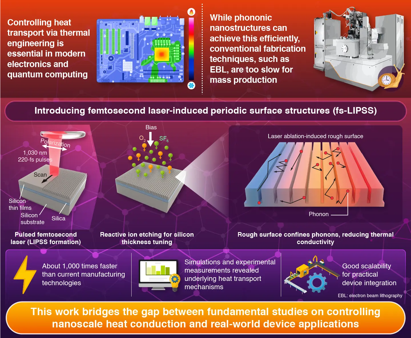
Controlling heat transport is among the most pressing challenges at the frontiers of electronics and quantum information technologies. As devices shrink in size while their power density grows, managing the intense heat they generate is essential for both performance and lifespan. One promising strategy to achieve this is phonon engineering, in which carefully designed phononic nanostructures are used to manipulate and scatter phonons—the quasiparticles of vibrational energy that conduct heat in many solids.
Despite the potential of phononic nanostructures for applications like nanoscale thermal insulation and energy conversion, they remain quite challenging to manufacture at industrial scales. Current high-resolution fabrication methods, such as electron-beam lithography (EBL), are inherently slow, complex, and expensive, rendering them unsuitable for mass production.
To address this issue, a research team led by Assistant Professor Byunggi Kim and Professor Kazuyoshi Fushinobu from the Department of Mechanical Engineering, Institute of Science Tokyo (Science Tokyo), Japan, in collaboration with Professor Masahiro Nomura from Institute of Industrial Science, The University of Tokyo, Japan, proposed a revolutionary technique to produce phononic nanostructures. Their latest paper, published online in the journal Advanced Functional Materials on December 03, 2025, demonstrates how their method could be the key to achieving laboratory-scale precision and industrial-scale throughput simultaneously.
The technique in question uses powerful high-speed lasers to carve small parallel grooves onto silicon/silica thin films through a process known as laser ablation. The parallel grooves are fabricated with periodicities and groove-bottom thickness comparable with the average distance travelled by the phonons. These highly uniform nanostructures, called femtosecond laser-induced periodic surface structures (fs-LIPSS), combined with the conventional dry-etching technique for silicon thickness tuning, greatly reduce the material's thermal conductivity, as demonstrated via the thermoreflectance measurements. To better understand the underlying physics, the researchers conducted a series of numerical simulations, which confirmed that the observed changes in thermal conductivity occur mainly because the periodic nanostructures limit phonons' average travel distance.
Notably, this novel fabrication approach achieves a throughput that is unprecedented in the field. The fs-LIPSS process was found to be more than 1,000 times faster than the conventional single-beam EBL, while maintaining the required nanoscale resolution. "The present results represent an important milestone toward translating fundamental research findings into real-world applications," highlights Kim. "We expect the proposed method to accelerate the development of advanced technologies in fields where thermal management is crucial, including high-performance computing, on-chip energy conversion, and quantum devices."
Overall, this work signals a shift toward the practical adoption of nanoscale thermal control. Since the fs-LIPSS technique is a maskless and resist-free process, it is inherently CMOS-compatible and highly scalable to wafer-level dimensions. This combination of speed and compatibility could make phonon engineering viable for mass production. "Our study establishes fs-LIPSS as a versatile platform for large-area thermal management and phonon engineering, and their functionality could be combined with optical and electronic properties, thereby aiding to establish a multifunctional platform," concludes Kim.
With any luck, this work will unlock new avenues for developing high-performance and energy-efficient electronic and quantum devices.
Reference
- Authors:
- Hiroki Hamma1, Roman Anufriev2,3, Kazuyoshi Fushinobu1*, Masahiro Nomura2*, and Byunggi Kim1*
*Corresponding authors
- Title:
- Scalable Thermal Engineering via Femtosecond Laser-Direct-Written Phononic Nanostructures
- Journal:
- Advanced Functional Materials
- Affiliations:
- 1Department of Mechanical Engineering, Institute of Science Tokyo, Japan
2Institute of Industrial Science, The University of Tokyo, Japan
3LIMMS, CNRS-IIS IRL 2820, The University of Tokyo, Japan


