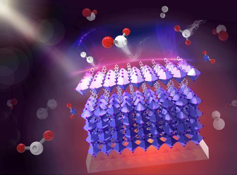
Artist's conception of a hybrid perovskite, in which a 3D perovskite crystal (bottom, in purple) is protected from water (red and white H2O molecules) by a 2D perovskite "cap" (top, in lavender).
Ming-Chun Tang, Siyuan Zhang/NIST
The crystal known as perovskite is a promising photovoltaic material for harnessing energy from sunlight. Perovskites have several advantages over silicon, the standard photovoltaic material currently used to make solar cells. Unlike silicon wafers, perovskites are lighter, smaller, and cheaper, as well as being physically flexible. Also, manufacturing them requires a smaller environmental footprint.
"Silicon is the primary semiconductor of photovoltaics because it has remarkable optoelectronic properties," said Ming-Chun Tang, a researcher at the National Institute of Standards and Technology (NIST). "However, using silicon wafers requires an expensive multi-step manufacturing process." In contrast, he continued, perovskites are simple to make in a laboratory, and perovskite solar cells have similar performance to silicon solar cells.
So why aren't they taking over the market?
There are commercial start-up companies working on making competitive perovskite photovoltaic devices. But perovskite solar cells have a significant challenge: They tend to be unstable, and their high efficiency quickly degrades. One way scientists have attempted to bolster the crystals is to dope them with alkali metals such as rubidium. But the field is young, and researchers are still studying how much dopant to use for the best photovoltaic performance.
In a new study, NIST scientists have conducted a comprehensive analysis on the impact of doping photovoltaic perovskites. The researchers found that for the perovskite solar cells they studied, a 5% concentration of rubidium provided the best performance. They also examined the impact of the increasingly popular practice of capping 3D perovskites with a protective 2D perovskite layer. The researchers published their work last month in Materials Advances.
They achieved their work using a technique that, to their knowledge, has not previously been applied to the problem of rubidium doping and 2D capping simultaneously.
Kristen Dill/NIST
"We have conducted a very thorough, holistic study of two recent promising discoveries - rubidium doping and 2D capping - to better understand the impact these discoveries have on perovskite technologies," said NIST researcher Christina Hacker. "We aren't the first to look at rubidium doping or 2D capping, but we are the first to really understand what role these discoveries have in a photovoltaic device."
People who can immediately use this information include industry researchers who are actively trying to make commercial perovskite solar energy devices.
Perovskites 101
Saying something is a perovskite crystal is a bit like saying something is a cupcake. The broad definition - "sweet bready thing topped with sweet creamy thing, wrapped in a paper cup" - doesn't specify flavors or colors. There is room to mix and match the components.
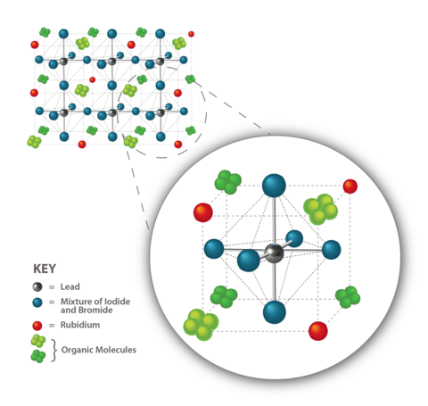
Similarly, a perovskite is a kind of crystal where many elements can be swapped out for different materials as long as the structural pattern remains. The classic perovskite crystal structure consists of a single atom with a positive charge (in this work, an atom of lead). Surrounding that atom is a crystal lattice made of negative atoms from the group of elements on the periodic table known as halogens (in this case, researchers used the negative ions iodide and bromide). Then that crystal is itself surrounded by other organic atoms with a positive charge, in this case molecules of carbon, nitrogen, and hydrogen. And the pattern repeats.
To utilize a perovskite crystal to convert sunlight into energy, researchers have to make the perovskite into a photovoltaic material. They sandwich the perovskite between two other layers: one that collects negative charge carriers and one that collects positive charge carriers. Negative carriers are electrons; positive carriers are referred to as "holes" and are places where an electron is missing.
In practice, sunlight hits the device and frees electrons from atoms within the crystal. Those newly freed electrons and "holes" migrate up or down to their respective collector layers. Once collected, the charges are ferried off to be used for work, such as lighting a lamp or starting a blender.
The term researchers use to describe a semiconductor's photovoltaic performance is "power conversion efficiency" (PCE). Silicon's PCE is around 26-27%. So far, scientists have found that perovskites have a PCE of as high as 25.5%, which is comparable. (The physical limit for photovoltaics is a PCE of 30%.)
But there are also major problems with perovskites as photovoltaic materials: Heat, light, and - in particular - moisture cause the crystal to degrade, which hurts performance. The crystal might start with a high efficiency of around 25%, but very quickly that efficiency can drop, over days or even hours. (One Swiss study found that when exposed to a relatively high humidity of 55%, the 3D perovskite device's performance decreased by 80% in just three days.) And this instability is one of the biggest problems with using perovskites as photovoltaic materials.
In their new study, the NIST researchers wanted to explore two of the solutions that the community is currently exploring to reduce perovskite degradation: moisture protection through "capping" the perovskite, and doping.
Better Than an Umbrella
Though perovskites occur naturally, they are more often created laboratories. Scientists first began studying them as possible solar energy material about a decade ago. Then a few years later, people began experimenting with different perovskite structures, referred to as 2D perovskites. But although these were much more stable than the traditional 3D crystals, their power conversion efficiency was much too low to make the 2D version a promising material in itself.
Then, just a couple of years ago, researchers began experimenting with combining 3D and 2D perovskites into a single device: a 3D crystal with a protective 2D "cap." They found this hybrid version takes a minor hit in its efficiency, but in exchange it becomes much more stable.
In their recent study, the NIST researchers examined the effect of a 2D cap on a device's performance. Their findings support what was suspected before: that the reason the 2D cap protects the 3D crystal from moisture is that it repels moisture. They found that a single drop of water on the 3D perovskite has a relatively low contact angle, indicating the water droplet has spread out for maximum contact with the crystal's surface. But a single drop of water on the hybrid perovskite has a much higher contact angle, indicating the water droplet has minimum contact with the surface.
"This means that the water is going to be less reactive with the perovskite material," Hacker said. "The 2D cap prevents the water from degrading the crystal structure, but it is thin enough that it does not lead to poor electrical properties."
How Much to Dope?
In the past few years, researchers have experimented with doping 3D perovskites with alkali metal ions such as rubidium, cesium, and potassium. These positive ions make the crystal more stable, possibly by preventing other components from moving within the lattice and segregating themselves.
Previous studies have shown that doping does improve device performance. But no one knew what the ideal doping concentration was.
The NIST researchers set out to do a thorough study that would determine the optimized doping concentration.
To find out which concentrations were best, the NIST researchers prepared several devices that fell into three categories: classic 3D perovskite, 2D film by itself, and hybrid 3D perovskite with a 2D cap. They doped the 3D and 2D/3D hybrid devices with various concentrations of rubidium ions: 0%, 1%, 5%, and 10%.
Then, they did a thorough analysis of the devices' performance and structure.
To see the electronic structure of the perovskite devices, they used ultraviolet photoelectron spectroscopy (UPS). Researchers shine ultraviolet light (which has wavelengths too small for the human eye to see) onto the devices. They then collect electrons emitted from the surface that tell them where the electrons are in the device. That allows them to measure what they would expect to see from the devices' electronic properties.
Then, to get information about the real-time charge-carrier activity of each perovskite, scientists used time-resolved terahertz spectroscopy (TRTS). This technique involves "activating" the sample by shining light on it, similar to the light that comes from the sun that would be converted into electricity by a solar cell. This light frees up the charge carriers, the electrons and holes. After this, researchers shine a beam of terahertz (THz) radiation - light whose wavelength is longer than the human eye can see - through the device.

Kristen Dill/NIST
How much THz radiation makes it to the other side tells them how many free charge carriers are in the device at the time, which gives the researchers insight into one of the critical processes that determine the photovoltaic performance of the material.
Finally, to uncover the physical location of the rubidium ions, the NIST researchers used x-ray photoelectron spectroscopy (XPS). Scientists shoot a beam of x-rays at the top layer of crystal, then measure the energy of the electrons that are ejected from the material. Based on the electron energies, they can identify each atom in the crystal. Then they remove that top layer of the crystal (by effectively shooting other atoms at it) and repeat the XPS measurement until every layer has been measured.
Using XPS in this way is "unique in the perovskite community," Tang said. This is one of the few studies so far that has shown exactly where the rubidium ions are, physically, in a 3D perovskite.
So which doping concentration turned out to yield the best performance?
"We found that 5% rubidium dopant gave us the highest perovskite solar cell efficiency," Tang said. Though more research is needed, it's believed that the reason for this improved solar cell efficiency is from enhancing carrier mobility, which may happen by making the crystal structure denser - effectively removing any "cracks."
Future Work
Tang said he hopes other research teams can use this information to better control the chemical composition distribution of the components of a 3D or hybrid 3D/2D perovskite crystal. He also hopes the work will provide members of the perovskite community with a simple strategy that they can use to design their own 3D/2D bi-layer perovskite architecture.
Meanwhile, Tang has turned his attention to studying lead-free perovskite materials.
"Lead-based materials were some of the first perovskite semiconductors ever studied, so for this paper they're great to look at because there's a lot of literature already on this topic," Hacker said. "But looking toward the future, the non-lead-based materials could be more environmentally friendly, and they could provide different optical and electronic properties as well."
Paper: M-C Tang, S. Zhang, T.J. Magnanelli, N.V. Nguyen, E.J. Heilweil, T.D. Anthopoulos, and C.A. Hacker. Unraveling the compositional heterogeneity and carrier dynamics of alkali cation doped 3D/2D perovskites with improved stability. Materials Advances. Published online December 11, 2020. DOI: 10.1039/D0MA00967A


