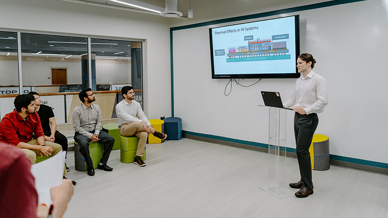
Graduate student Michael Smith presents to students working in advanced semiconductors packaging at the Chiminski Family Collaborative Research Hub. Purdue announced the Institute of Advanced System Integration and Packaging, renewing focus on essential areas of semiconductor chip manufacturing. (Purdue University photo/Kelsey Lefever)
Purdue collaborates with Cadence, imec, SRC, Osaka University to bolster rapid technology development in U.S.
WEST LAFAYETTE, Ind. – Purdue University is working toward the future in microelectronic product development with the creation of the Institute for Advanced System Integration and Packaging (ASIP) to enable faster designing and building of microelectronic systems.
The new institute, announced Wednesday (Oct. 18), highlights Purdue's established research in system integration and puts new focus on advanced packaging at the university. Chip packaging ensures the functionality and reliability of a system, as multiple chips are connected electrically. Advanced packaging aims to revolutionize packaging by enabling complex functionality while reducing cost.
Additional Information
- Purdue establishes permanent presence next to NSWC Crane for future of national defense and semiconductors
- Second funding round delivers $19 million to Purdue-led microelectronics workforce development program
- Purdue signs landmark U.S.-Japan agreement in semiconductors at G7 summit
"Today, the U.S. only has 3% of the global packaging capability, but advanced packaging presents the U.S. with new opportunities. ASIP is the latest chapter of leadership for Purdue as the semiconductor industry seeks new ways to advance system performance and reshore packaging," said Mark Lundstrom, Purdue's chief semiconductor officer. "Purdue will lead the charge with a foundation of strong partners and a growing list of future collaborators."
"ASIP will draw on the strengths of Purdue to accelerate microelectronic system integration and technology development while producing the high-tech workforce needed," said Indiana Gov. Eric Holcomb. "Strong partnerships with companies, research organizations and other universities will help establish Indiana as a major center of innovation in this critical technology. We look forward to working with ASIP to bring national and international microelectronics companies to Indiana."
Purdue is working with Cadence Design Systems, one of its many U.S. and global semiconductor partners, to establish ASIP. Cadence is a leader in electronic systems design, with more than 30 years of computational software expertise to support and bolster the system design goals of ASIP.
"Purdue University is a nationally recognized leader in academic excellence and microelectronics workforce development," said Tom Beckley, senior vice president and general manager in the Custom IC & PCB Group at Cadence. "We are excited to collaborate with Purdue to ensure that the next generation of advanced package engineers are equipped to design complex heterogeneous 3D-ICs while addressing multiphysics analysis challenges including power, thermal integrity, signal integrity, electromagnetics and mechanical stress. It is critical that graduating engineers are highly familiar with industry-leading commercial tools, thereby providing students, their future employers and the U.S. competitive advantage."
Ganesh Subbarayan, ASIP director and Purdue's James G. Dwyer Professor of Mechanical Engineering, said the institute's creation will build a foundation for advanced packaging and system integration that has been neglected for too long. That makes ASIP a valuable contributor to the U.S. microelectronics industry moving forward.
"System integration and advanced packaging are huge opportunities for Purdue and a big priority for the nation right now," Subbarayan said. "With ASIP, we envision designing a chip system from the beginning, envisioning a system to consist of multiple chips that are interconnected and with an advanced material that avoids having to put everything on a single chip."
Subbarayan also is co-director of the Semiconductor Research Corporation (SRC)-funded Center for Heterogenous Integration Research in Packaging (CHIRP). He said the university is one of a few with a strong focus on packaging, with four centers researching various aspects.
"Very few universities have established educational programs in packaging, which is an area of such critical need," Subbarayan said. "We have developed a unique educational curriculum for semiconductors at Purdue, including packaging."
SRC, a consortium of the top global semiconductor companies and the leading sponsor of microelectronics-related research in U.S. academia, will partner with Purdue in the ASIP institute along with imec, a premier research center for lab-to-fab semiconductor and advanced packaging research, and Osaka University, Japan's premier research university for 3D integration and advanced packaging.
- "SRC is a major sponsor of research and workforce development efforts at Purdue University through its funding of CHIRP as well as CBRIC, COCOSYS and NEW LIMITS centers," said Todd Younkin, SRC president and CEO. "We look forward to partnering with the ASIP institute as we broaden and deepen our engagement with Purdue University."
- Dave Henshall, SRC vice president of business development, said, "The formation of ASIP is very timely. Purdue researchers have played a leadership role in developing the SRC MAPT road map for the nation, and we look forward to building upon that in ways that will energize advanced packaging design and manufacturing in the U.S."
- "We applaud the establishment of the Institute for Advanced System Integration and Packaging," said Luc Van den hove, president and CEO of imec. "To cope with the increasing functionality of future systems, advanced packaging solutions such as 3D integration have become indispensable. To realize these complex systems, in-depth understanding and knowledge of advanced packaging is key, including access to modeling and simulation. With our long track record in advanced R&D on semiconductor and system integration and packaging and our mission to drive the semiconductor industry forward by collaborating with the entire value chain, we look forward to partnering with ASIP to build up the necessary knowledge. An initiative like ASIP is important to enabling the CHIPS Act and propelling the semiconductor industry forward."
- "Purdue and Osaka University are natural partners with their leading research roles in the area of advanced packaging," said Katsuaki Suganuma, director of the Flexible 3D Integration Laboratory at Osaka University. "Our research strengths are complementary. We are actively engaged in creating collaborative opportunities between companies of our two countries to secure the global supply chain."
ASIP tackles two aspects of chip production that have become integral parts of the industry.
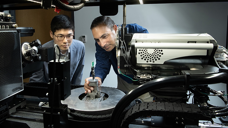 Nikhilesh Chawla, the Ransburg Professor of Materials Engineering at Purdue University, and Min Cho, a doctoral student in his research group, prepare to examine a novel microstructural fingerprint for microelectronic security applications with a 3D X-ray microscope at the Flex Lab in Discovery Park District at Purdue. (Purdue University photo/John Underwood)
 System integration focuses on the design activity that precedes chip fabrication, looking at ways to avoid putting everything on a single chip by creating a system that interconnects multiple smaller chips, or chiplets. Future applications will require novel system integration solutions to achieve performance, power and cost trade-offs while ensuring efficiency.
Advanced packaging addresses the escalating cost of building chips by putting several chiplets as close together as possible to achieve the function of a single larger chip. This research includes looking at reducing heat production by design, heat removal strategies, ensuring fail-free functioning, and enabling sustainable manufacturing.
The need for chips in areas from computing, mobile communications and vehicles to defense and biological applications requires future advanced system integration and packaging like that represented by Purdue's research.
Purdue is a national leader in microelectronics materials, devices, chip design, tool development, manufacturing, packaging and sustainability, spanning the semiconductor ecosystem in software and hardware with long-standing faculty excellence.
Strategic initiatives in semiconductors, such as the first comprehensive Semiconductor Degrees Program, which was announced before the CHIPS and Science Act passed in 2022, are intended to prepare a next-generation workforce for industry. Economic development and research collaboration followed as well, including from Skywater, MediaTek and Belgium-based imec.
As part of the Purdue Computes initiative, Purdue's growing semiconductor innovation ecosystem includes $49 million in new facilities and tools for the Birck Nanotechnology Center, which will also be accessible by Ivy Tech Community College, Indiana's statewide community college and a local partner with Purdue in developing next-level workforce and brain gain strategies for Indiana.
The Indiana-led proposal "Silicon Crossroads" was announced Sept. 20 by the U.S. Department of Defense as one of eight Microelectronics Commons Hubs selected out of over 80 proposals across the country. The Naval Surface Warfare Center, Crane Division (NSWC Crane), in Indiana will manage the program. Purdue will collaborate with many consortium members in the coming years.
Purdue announced in September the creation of Purdue@Crane, a permanent Purdue presence for national security research collaboration with NSWC Crane, including participation in the WestGate Foundry with companies such as Everspin Technologies and NHanced Semiconductors.


