The era defined by Moore's Law - which has delivered an astonishing billion-fold increase in transistor density since 1958 - is reaching its physical and economic boundaries, creating new challenges for the future of computing. At Berkeley Lab, researchers are pioneering solutions that transcend conventional scaling limitations while addressing the growing demands of data-centric computing and our nation's critical infrastructure needs. Berkeley Lab researchers have long partnered with industry, universities, and national labs to develop new materials and techniques for smaller, faster, and more energy-efficient microelectronics. Because of these advances, it could be decades before these fundamental technologies run out of room for improvement
Here are six ways Berkeley Lab is advancing microelectronics of the future.
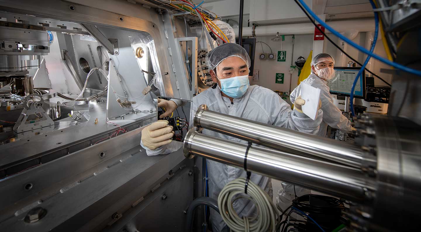
Ryan Miyakawa (left) checks the alignment of light as it enters the CXRO high-resolution camera while Martin Izquierdo controls the optics that guide the light into the chamber. (Credit: Thor Swift/Berkeley Lab)
Pushing the Boundaries of Moore's Law for Smaller, Faster Devices
After decades of research and development, extreme ultraviolet (EUV) lithography has recently reached the point of high-volume semiconductor manufacturing, marking a significant technological breakthrough. Berkeley Lab's Center for X-ray Optics (CXRO) has played an instrumental role in this achievement, working directly with chipmakers to develop tools to overcome longstanding challenges in EUV resist performance and mask defects. As EUV lithography advances to its next generation, CXRO continues to address ongoing obstacles in optics, masks, and materials, enabling the creation of even smaller semiconductor features for future electronics.
Bruno La Fontaine, Director of the Center for X-ray Optics (CXRO), speaks on how the CXRO supports the microchip industry.
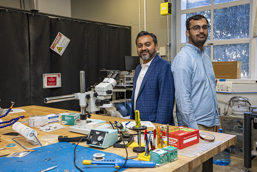
Berkeley Lab scientists Sayeef Salahuddin (left) and Nirmaan Shanker in the lab. Their groundbreaking microcapacitors could enable on-chip energy storage in electronic devices. (Credit: Marilyn Sargent/Berkeley Lab)
Record-Breaking Capacitors for Next-Gen Microchips
The push to develop smaller and more energy-efficient electronic devices has led researchers to explore integrating energy storage directly onto microchips. This integration would minimize energy losses that occur during power transmission between device components. Effective on-chip energy storage necessitates high energy density, compact size, and rapid power delivery - requirements that current technologies cannot fulfill. Berkeley Lab scientists have addressed this challenge by creating groundbreaking microcapacitors with ultrahigh energy and power density, potentially transforming on-chip energy storage for electronic devices. These microcapacitors utilize engineered thin films and leverage materials and fabrication techniques commonly used in chip manufacturing.
Pioneering New Light-Based Approaches for Computing
Recent breakthroughs at Berkeley Lab demonstrate how light-manipulating materials can enable smaller, faster microchip components for next-generation computers. In one advance, researchers are working on improving the performance of optoelectronic devices - from scientific tools to smartphone cameras. Inspired by the human eye, the researchers aim to convert photons directly into information instead of images, making the process more efficient. This could reduce the energy currently used to transmit and analyze images, enhancing device performance. Another Berkeley Lab team developed a new optical computing material from photon-avalanching nanoparticles, which could enable the fabrication of optical memory and transistors at dimensions comparable to current microelectronics, offering a path toward realizing smaller, faster components for next-generation computers.
Accelerating Microelectronics Innovation by Experimenting in the Digital Realm
Berkeley Lab is accelerating low-power microelectronics innovation through advanced computer modeling, reducing both time and expense for discovery. Researchers developed the FerroX framework to design new ferroelectric-based transistors, optimizing performance through detailed nanoscale simulations. Complementing this, the code package ARTEMIS enables rapid prototyping of microelectronic circuitry by accurately modeling electromagnetic signals in a wide range of materials and conditions, including superconductors and magnetic materials. These open-source digital tools empower researchers to innovate more efficiently and with greater flexibility, driving the development of next-generation microelectronics.
Taking Device Miniaturization to the Nanoscale
Over the past decade, Berkeley Lab researchers have achieved nanoscale breakthroughs in microelectronics, expanding the realm of possibility for device miniaturization. In 2016, they created a one-nanometer gate transistor, breaking a size barrier previously thought to be set by the laws of physics and potentially paving the way for smaller, faster, and more energy-efficient transistors. More recently, they developed a one-atom-thin 2D magnet, a remarkable material that could lead to new applications in computing and electronics, including high-density, compact spintronic devices such as next-generation memories. These record-breaking achievements, enabled by advanced capabilities at the Molecular Foundry and the Advanced Light Source, could pave the way for ultra-low-power, next-generation microelectronic devices.
Groundbreaking Transistor Architecture Foreshadowed Microelectronics Evolution
As the microelectronics industry moves to adopt gate-all-around transistor designs in next-generation smartphones, groundbreaking research at Berkeley Lab demonstrated an innovative approach to creating these advanced structures nearly 20 years ago.
The technology - called gate-all-around field-effect transistors (GAA-FET) - represents a key architectural advance for packing billions more transistors into the tiny microchips that are found in smartphones and laptops. The "gate-all-around" design enhances control over the transistor channel, leading to better performance and lower power consumption. While industry is now implementing GAA-FET through traditional top-down fabrication, Berkeley Lab's early bottom-up approach showed the potential of this geometry using chemical synthesis to achieve these complex structures.


