In the field of 2D electronics, the norm used to be that graphene is the main protagonist and hexagonal boron nitride (hBN) is its insulating passive support.
An international team of researchers, affiliated with UNIST, has made a discovery that might change the role of hBN. They have reported that stacking of ultrathin sheets of hBN in a particular way creates a conducting boundary with zero bandgap. In other words, the same material could block the flow of electrons, as a good insulator, and also conduct electricity in a specific location. Published in the journal Science Advances (IF: 12.804), this result is expected to raise interest in hBN by giving it a more active part in 2D electronics.
This breakthrough has been led by Professor Zhonghoon Lee (School of Materials Science and Engineering), who also serves as a group leader of the Center for Multidimensional Carbon Materials (CMCM) within the Institute for Basic Science (IBS, South Korea) at UNIST.
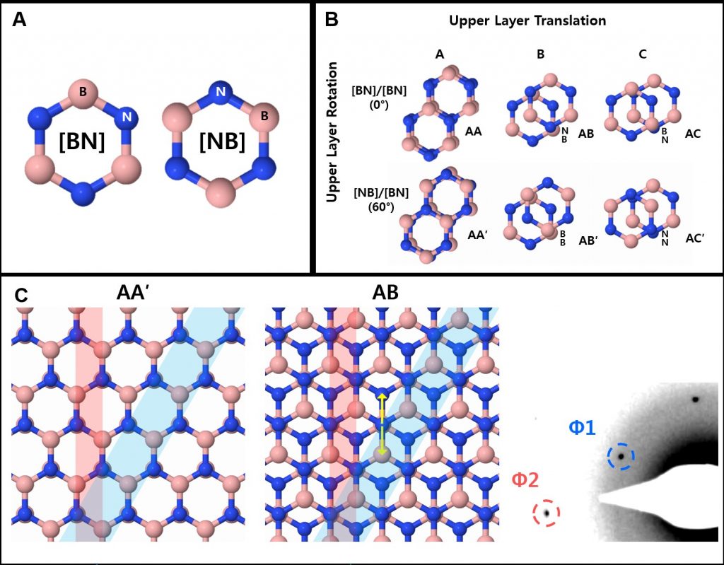
▲ Figure 1: A layer of hexagonal boron nitride has the shape of a chicken wire, and is formed by the alternation of boron (B, pink) and nitrogen (N, blue). Depending on how the layers are piled up together, the material assumes different arrangements: AA, AB, AC, AA′, AB′, and AC′. The team achieved and studied a AA′/AB stacking boundary for the first time.
Similarly to graphene, hBN is a 2D material with high chemical, mechanical and thermal stability. hBN sheets resemble a chicken wire, and are made of hexagonal rings of alternating boron and nitrogen atoms, strongly bound together. However, unlike graphene, hBN is an insulator with a large bandgap of more than five electronVolts, which limits its applications.
"In contrast to the wide spectrum of proposed applications for graphene, hexagonal boron nitride is often regarded as an inert material, largely confined as substrate or electron barrier for 2D material-based devices. When we began this research, we were convinced that reducing the bandgap of hBN could give to this material the versatility of graphene," says Hyo Ju Park, the first author of the study.
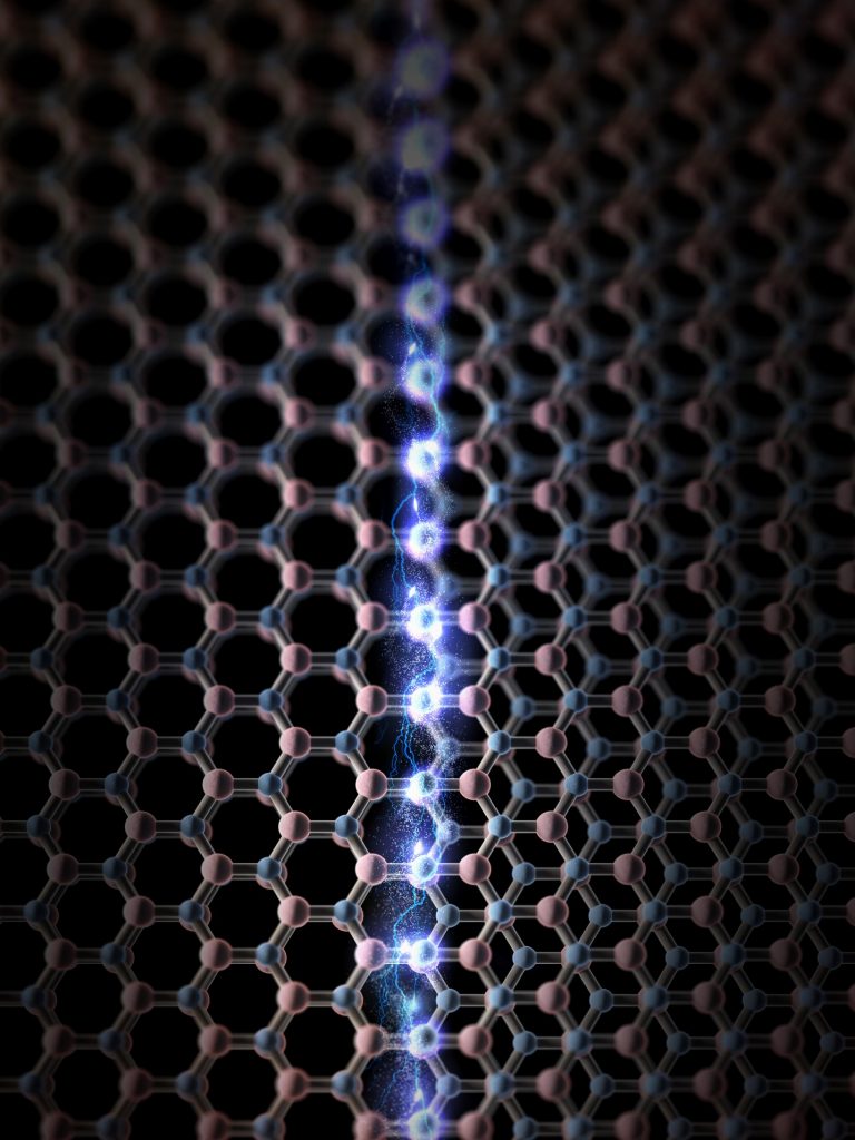
▲ Figure 2: A conducting channel forms at the stacking boundary of hexagonal boron nitride (hBN) sheet which appears to be stitched together with oblong hexagonal rings. It joins an arrangement of all nitrogen atoms lying above boron atoms, and all boron atoms lying above nitrogen atoms in perfectly aligned positions (left side of the channel) and another configuration where half of the atoms lie over the center of the rings of the lower sheet, and the other half overlap with the atoms underneath (right side of the channel).
Several attempts to lower the bandgap of hBN have been mostly ineffective because of its strong covalent boron-nitrogen bonds and chemical inertness. IBS researchers in collaboration with colleagues of Ulsan National Institute of Science and Technology (UNIST), Sejong University, Korea, and Nanyang Technological University, Singapore, managed to produce a particular stacking boundary of a few hBN layers having a bandgap of zero electronVolts.
Depending on how the hBN sheets are piled up, the material can assume different configurations. For example, in the so-called AA′ arrangement, the atoms in one layer are aligned directly on the top of atoms in another layer, but successive layers are rotated such that boron is located on nitrogen and nitrogen on boron atoms. In another type of layout, known as AB, half of the atoms of one layer lie directly over the center of the hexagonal rings of the lower sheet, and the other atoms overlap with the atoms underneath.
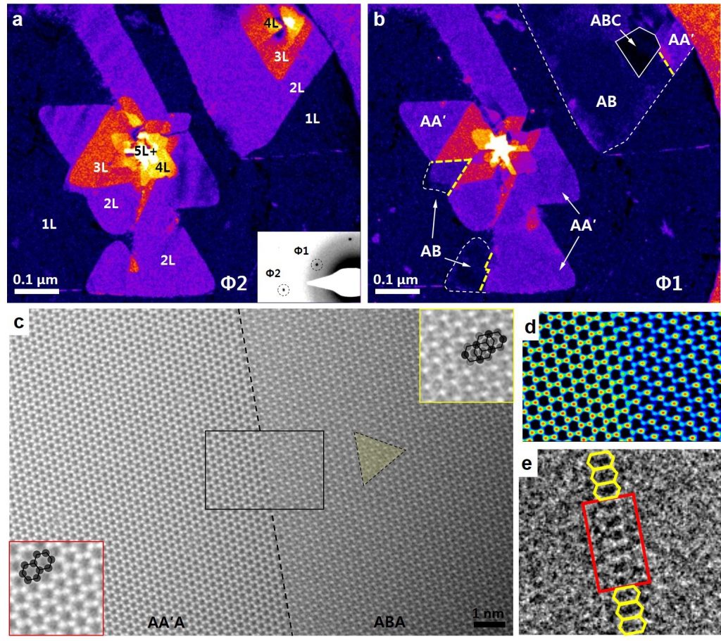
▲ Figure 3: Transmission electron microscopy images of few-layer hexagonal boron nitride with atomically sharp AA'/AB stacking boundaries. The zero bandgap channels between AA′ and AB are indicated with yellow dashed lines in (b), and represented at high resolution also in (c), (d) and (e).
For the first time, the team has reported atomically sharp AA′/AB stacking boundaries formed in few-layer hBN grown by chemical vapor deposition. Characterized by a line of oblong hexagonal rings, this specific boundary has zero bandgap. To confirm this result, the research performed several simulations and tests via transmission electron microscopy, density functional theory calculations, and ab initio molecular dynamics simulations.
"An atomic conducting channel expands the application range of boron nitride infinitely, and opens new possibilities for all-hBN or all 2D nanoelectronic devices," points out Professor Lee, the corresponding author of the study.


