Cornell researchers have uncovered a nearly invisible culprit hindering the development of next-generation, high-power electronics: a microscopic layer of carbon contamination, often left behind by air exposure and fabrication techniques, that impairs electrical flow in devices made with gallium oxide. They have also found a solution.
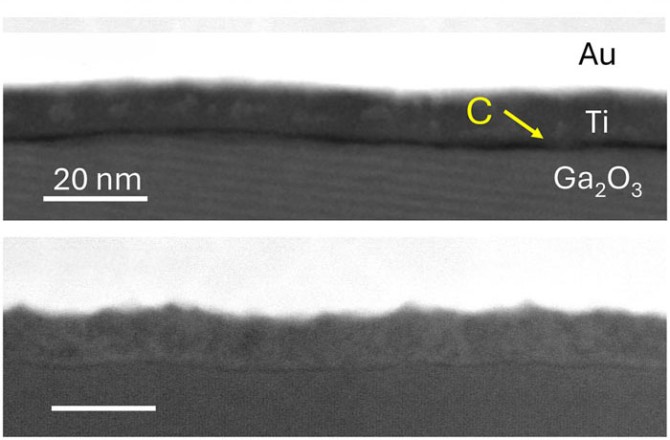
Scanning transmission electron microscopy cross-sectional images of the titanium and beta gallium oxide interface. The top sample is non-conductive and shows an approximately 1 nanometer thick carbon contamination layer, labeled C, at the interface, which is not observed in the linear ohmic contact sample at the bottom.
A study published June 20 in the journal Applied Physics Letters is among the first to directly visualize this nanometer-thin barrier that can occur when metals are patterned onto semiconductors, an essential interface for getting current in and out of electronic devices. When these contacts have resistance, device performance suffers.
The challenge is especially pronounced in beta gallium oxide, a semiconductor material with an ultra-wide band gap that could one day allow devices like electric vehicles and grid infrastructure to more efficiently handle higher voltages.
"It's been a problem in the gallium oxide field for quite some time," said Naomi Pieczulewski, a doctoral student in materials science and engineering and the study's co-lead author. "Sometimes you get good conduction and sometimes you get absolutely no conduction at all, and no one could really pinpoint why."


