The atomic thick two-dimensional (2D) materials are promising for many applications, such as faster and energy-saving electronic devices, more efficient catalysts, and high energy density batteries. To fully utilize the advantages of these 2D materials, the ability to synthesize high-quality, large-area 2D materials in a single crystalline form is essential. Although the technologies of synthesizing large-area three-dimensional (3D) single crystals (i.e., Single crystalline silicon ingots used in the semiconducting industry) have been well established, the growth of 2D single crystals is still a challenge. This is because large-area 2D materials must grow on a substrate, and the selection of an appropriate substrate is the key.
A research team, led by Distinguished Professor Feng Ding (Department of Material Science and Engineering) from the Center for Multidimensional Carbon Materials (CMCM), within the Institute for Basic Science (IBS) at UNIST, recently provides a general solution of synthesizing 2D single crystals-using properly selected substrates with both flat terraces and step edges, namely high-index surfaces.
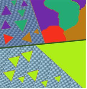
Figure 1. Illustration of 2D materials grown on an ultra-flat low-index surface (above) or a high-index surface with terraces and step edges (bottom).
As illustrated in Figure 1, an ideal high-index surface is composed of low-index ultra-flat terraces and parallel step edges. These step edges serve as active sites for the nucleation of 2D materials and lead to a unidirectional alignment of the grown 2D materials, and these aligned 2D materials can merge into a large area single crystal. On the contrary, the grown 2D materials on the ultra-flat low-index surface usually presented multiply orientations and these 2D materials will finally merge into a polycrystalline film.
Among the infinite number of high-index surfaces, which one is the best to template the growth of a 2D material? To answer this question, using hBN growth on Cu surfaces as an example, the authors systematically explored the mechanism of 2D materials epitaxial growth on various ideal high-index surfaces. The developed theory allows us to predict the alignment of a 2D material on an arbitrary substrate and, as shown in Figure 2, it is found that all the existing experimentally measured alignments of hBN on eight different high-index Cu surfaces agree with the theoretical predictions perfectly.
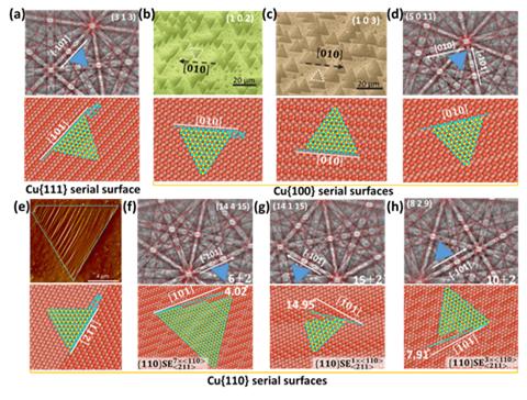
Figure 2. Comparison of experimental and theoretical results. (a) hBN growth on a Cu{111}serial high-index surface, Cu(313). (b-d) hBN growth on Cu{100} serial high-index surfaces, Cu(102), Cu(103), Cu(5 0 11). (e-h) hBN growth on Cu{110} serial high-index surfaces, a vicinal Cu(110), Cu(14 4 15), Cu(14 1 15), Cu(8 2 9).
Technically, most substrates are not ultra-flat, and their roughness must be considered. The authors also revealed that the surface roughness will result in curved step edges and thus affect the alignment of the 2D material. Beyond our intuition, the high-index surfaces with a high density of step-edges were found more robust for templating the epitaxial growth of 2D single crystals. "Our theory clearly showed that previous experimental efforts, that using low-index or near-low-index substrates to grow high-quality 2D materials are not effective, whereas those substrates far from the low-index surfaces should be considered more seriously," Leining Zhang, the first author of the study explained.
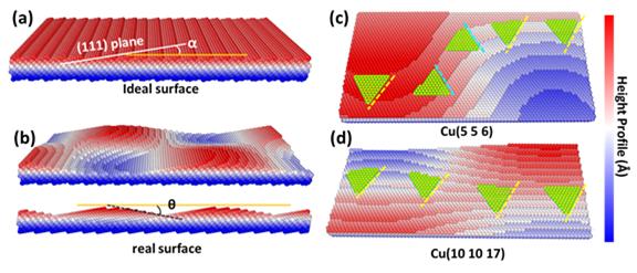
Figure 3. (a) Atomic configuration of an ideal high-index surface. (b) The atomic illustration of a rough high-index surface. (c-d) The alignment of hBN islands on two high index surfaces, namely Cu(5 5 6) and a Cu(10 10 17), with the same surface roughness, from which we can see that an hBN island-grown on the rough Cu(5 5 6) surface have two possible alignments but those grown the rough Cu(10 10 17) surface are unidirectionally aligned.
The theoretical study provides a deep guideline for the synthesis of 2D single crystals and thus is highly inspiring for the materials society. Besides hBN growth on Cu surfaces, the main conclusions can be applied to understand the growth behaviors of various 2D materials. "With the assistance of our theory, we expect that various 2D single crystals could be available for both experimental studies and industrial applications in 5 to 10 years," said Professor Ding.
The findings of this study have been published in the July 2021 issue of Advanced Functional Materials. This study has been supported by the Institute for Basic Science (IBS).
Journal Reference
Leining Zhang, Peng Peng, and Feng Ding, "Epitaxial Growth of Two-dimensional Materials on High-Index Substrate Surfaces," Adv. Funct. Mater., (2021).


