Cornell researchers have used high-resolution 3D imaging to detect, for the first time, the atomic-scale defects in computer chips that can sabotage their performance.
The imaging method, which was the result of a collaboration with Taiwan Semiconductor Manufacturing Company (TSMC) and Advanced Semiconductor Materials (ASM), could touch almost every form of modern electronics, from phones and automobiles to AI data centers and quantum computing.
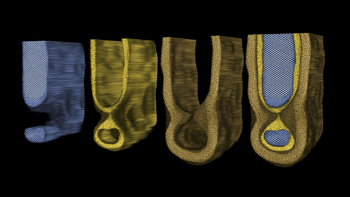
This image shows the silicon, silicon dioxide and hafnium oxide layers inside a transistor channel.
The research published Feb. 23 in Nature Communications. The lead author is doctoral student Shake Karapetyan.
"Since there's really no other way you can see the atomic structure of these defects, this is going to be a really important characterization tool for debugging and fault-finding in computer chips, especially at the development stage," said David Muller, the Samuel B. Eckert Professor of Engineering in the Cornell Duffield College of Engineering, who led the project.
Tiny defects have been a long-standing challenge for the semiconductor industry, especially now, as the technology has grown increasingly complex while the components have shrunk in size to the atomic scale.
The focus of the study, and the heart of the computer chip itself, is the transistor: the little switch through which electrical current flows via a channel that gets opened and shut by an electrical gate.
"The transistor is like a little pipe for electrons instead of water," Muller said. "You can imagine, if the walls of the pipe are very rough, it's going to slow things down. And so measuring how rough the walls are and which walls are good and which walls are bad is now even more important."
'It was like flying biplanes. And now you've got jets.'
Muller has a unique insight into the design of semiconductors. From 1997 to 2003, he worked in the research and development division of Bell Labs - where transistors were invented - exploring the physical limits that dictate just how tiny a transistor could get.
After their introduction in the mid-20th century, transistors were initially built like suburbs: flat and sprawling outward, according to Muller. Over time, as the chips ran out of horizontal real estate, designers started to stack transistors vertically, in three dimensions, like apartment blocks.
"The problem is these 3D structures are smaller than the size of a virus. And these days, it's a lot smaller. It's more like a molecule-in-the-cell kind of scale," Muller said.
A single high-performance chip can now contain billions of transistors. But as they've shrunk in size, the technology has become more difficult to troubleshoot.
"These days, a transistor channel can be only about 15 to 18 atoms wide, which is super, super tiny, and they're extremely intricate," Karapetyan said. "At this point, it matters where every atom is, and it's really hard to characterize."
At Bell Labs, Muller and fellow scientist Glen Wilk '90, who is now vice president of technology at ASM, tried replacing silicon dioxide - the prevailing gate material, which leaked too much current at small scales - with hafnium oxide. Within a few years, Muller and Wilk departed Bell Labs, but their work continued to reverberate with semiconductor companies, and hafnium oxide soon became the industry standard for computers and cell phones in the mid-aughts.
"The papers we published on how to use electron microscopes to characterize these materials, I can tell you, a lot of the semiconductor folks had read those very, very carefully," said Muller, who co-directs the Kavli Institute at Cornell for Nanoscale Science and the Cornell Center for Materials Research (CCMR). "When we got back into this project, that was very clear. And the microscopy has gone a very long way. Back then, it was like flying biplanes. And now you've got jets."
The jet, in this case, is electron ptychography, a computational imaging method in which an electron microscope pixel array detector (EMPAD) - a technology co-developed by Muller's group - is used to collect detailed scattering patterns of electrons after they pass through the transistors. By comparing how these patterns change from one scan position to the other, scientists can reconstruct an image with extraordinary clarity. The detector is so precise, it has enabled the highest resolution images in the world, showing atoms in unprecedented detail, as recognized by Guinness World Records.
'Mouse bites'
More than 25 years after their last joint project, and with the support of TSMC and its Corporate Analytical Laboratories group, Muller's team and Wilk decided to collaborate again and use the EMPAD to peer inside modern semiconductors.
"You can think of this imaging technique like solving a massive puzzle, both in terms of taking the experimental data and doing the computational reconstruction," Karapetyan said.
When all the data was collected and reconstructed, and the position of atoms had been tracked, the researchers were able to detect interface roughness in the channels - revealing what Karapetyan termed "mouse bites." The roughness arose from defects that formed during the optimized growth process. Sample structures, grown at nanoelectronics hub Imec, were the ideal way to test the imaging method.
"Fabrication of modern devices takes hundreds, if not thousands, of steps of chemical etching and deposition and heating, and then every single step does something to your structure," Karapetyan said. "Before you used to look at projective images to try to figure out what was really going on. Now you have a direct probe to actually see after every single step and have a better grasp of, oh, I put the temperature this high, and then this is what it looks like."
The new imaging capability could potentially impact almost anything with a modern computer chip, from cellphones to laptops and data centers, and could be a boon for debugging next-generation technologies such as quantum computers, which require extraordinary structural control of materials that is still not fully understood.
"I think there's a lot more science we can do now, and a lot more engineering control, having this tool," Karapetyan said.
Co-authors include Steven Zeltmann, staff scientist at Platform for the Accelerated Realization, Analysis and Discovery of Interface Materials (PARADIM); and Ta-Kun Chen and Vincent Hou of TSMC.
The research was funded by TSMC. Support for the microscopy facilities was provided by CCMR and PARADIM, which are funded by the National Science Foundation.


