Scientists at Tokyo Institute of Technology develop a 3D functional interposer—the interface between a chip and the package substrate—containing an embedded capacitor. This compact design saves a lot of package area and greatly reduces the wiring length between the chip's terminals and the capacitor, allowing for less noise and power consumption. Their approach paves the way to new semiconductor package structures with greater miniaturization.
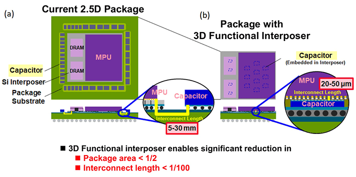
Figure 1. State-of-the-art 2.5D package design versus 3D functional interposer design
The new interposer design with an embedded capacitor provides a notable reduction in area requirements and interconnect length, leading to lower wiring resistance and parasitic capacitance. MPU: Microprocessing unit; DRAM: Direct random-access memory.
Electronics started big size-wise but have only grown smaller and more compact over time. Today, even smartphones outperform the bulky computers from the 1980s by orders of magnitude. Unfortunately, this accelerating trend in performance and scale is bound to slow down considerably as the materials and designs we use approach their physical limits. To overcome such problems, it is critical to think out of the box and come up with designs that address technological bottlenecks.
Over the last decade, progress in an essential passive component in electronics, the capacitor, has stagnated in some regards. Although we can fabricate much smaller capacitors than ever before, their actual capacity per unit area hasn't been improving as much. We need ways to make capacitors occupy less space while preserving their performance.
But what if we could integrate capacitors inside another element commonly used in modern circuits: the interposer? At Tokyo Institute of Technology, Japan, a team of scientists led by Professor Takayuki Ohba have committed to developing technologies to sustain the scaling of semiconductor circuits. In their latest study, which will be presented at the Proceedings of the 2021 IEEE Electronic Components and Technology Conference, they demonstrated that silicon interposers—the planar interface that holds and vertically connects an integrated chip with a circuit package or another chip—can be made into functional capacitors, thus saving up considerable space, and bringing along a ton of benefits.
In modern "2.5D" packages, chips such as DRAMs and microprocessors sit atop interposers with through-silicon vias, vertical conducting tunnels that bridge the connections in the chips with solder bumps on the package substrate. Capacitors are placed on the package substrate close to the components they serve, and a connection between their terminals and those of the chip has to be made, spanning 5-30 mm (Figure 1a). This layout not only increases the necessary package substrate area, but also causes problems such as high wiring resistance and noise due to the long interconnections.
In stark contrast with this design, the team at Tokyo Tech cut the middleman and directly made the interposer be the silicon capacitor (Figure 1b). They achieved this through a novel fabrication process in which the capacitive elements are embedded inside a 300 mm silicon piece using permanent adhesive and mold resin. The interconnects between the chip and the capacitor are made directly with through-silicon vias and without the need for solder bumps. "Our bumpless 3D functional interposer enables a notable reduction in package area of about 50% and an interconnect length a hundred times shorter," remarks Ohba.
The researchers also managed to cleverly avoid the two most common problems of bumpless chip-on-wafer designs, namely warping in the wafer due to the resin and misplacement errors due to void pockets in the adhesive. Through testing and theoretical calculations, they determined their functional interposer allowed for a wiring resistance about a hundred times lower than conventional designs, as well as a lower parasitic capacitance. These features could enable the use of lower supply voltages, leading to lower power consumption. "The chip-on-wafer integration technology we are developing will open up new routes in the evolution of semiconductor package structures," concludes Ohba excitedly. Overall, this study is a perfect example of the creative leaps that are needed if the accelerating march of technology is to be maintained.
Reference
Authors : |
Tatsuya Funaki1,2, Yoshiaki Satake1,2, Kyosuke Kobinata1,3, Chih-Cheng Hsiao4, Hitoshi Matsuno1,2, Shunsuke Abe1,2, Youngsuk Kim1,3, Takayuki Ohba1
|
Title of original paper : |
Miniaturized 3D Functional Interposer Using Bumpless Chip-on-Wafer (COW) Integration with Capacitors |
Session : |
Session 5: Technologies for Advanced Substrates and Flip-Chip Bonding |
Conference : |
|
Affiliations : |
1 Tokyo Institute of Technology 2 Murata Manufacturing Co., Ltd. 3 DISCO CORPORATION 4 Industrial Technology Research Institute |


