Novel University of Rochester solution paves the way for cutting-edge photonics.
One of the most tedious, daunting tasks for undergraduate assistants in university research labs involves looking hours on end through a microscope at samples of material, trying to find monolayers.
These two-dimensional materials-less than 1/100,000th the width of a human hair-are highly sought for use in electronics, photonics, and optoelectronic devices because of their unique properties.
"Research labs hire armies of undergraduates to do nothing but look for monolayers," says Jaime Cardenas, an assistant professor of optics at the University of Rochester. "It's very tedious, and if you get tired, you might miss some of the monolayers or you might start making misidentifications."
Even after all that work, the labs then must doublecheck the materials with expensive Raman spectroscopy or atomic force microscopy.
Jesús Sánchez Juárez, a PhD student in the Cardenas Lab, has made life a whole lot easier for those undergraduates, their research labs, and companies that encounter similar difficulties in detecting monolayers.
The breakthrough technology, an automated scanning device described in Optical Materials Express, can detect monolayers with 99.9 percent accuracy-surpassing any other method to date.
At a fraction of the cost. In far less time. With readily available materials.
"One of the main objectives was to develop a system with a very small budget so that students and labs can replicate these methodologies without having to invest thousands and thousands of dollars just to buy the necessary equipment," says Sánchez Juárez, the lead author of the paper.
For example, the device he created can be replicated with an inexpensive microscope with a 5X objective lens and a low-cost OEM (original equipment manufacturer) camera.
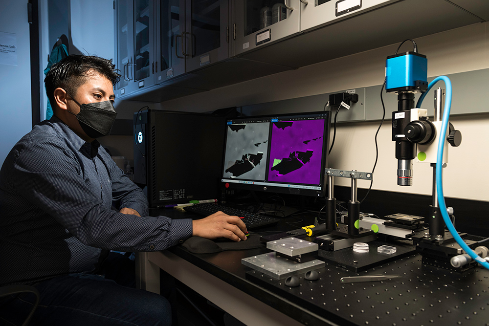
Jesús Sánchez Juárez, a PhD student in the lab of Jaime Cardenas, has made it easier to detect monolayers-two-dimensional materials less than 1/100,000 the width of a human hair-which are highly sought for use in electronics, photonics, and optoelectronic devices because of their unique properties. Sánchez Juárez combined an inexpensive microscope with a 5X objective lens and a low-cost camera, shown at far right, with an artificial intelligence neural network, to detect, and then process images of monolayers, as shown in green on his computer screen. (Photo by J. Adam Fenster/University of Rochester)
A creative adaptation of an AI neural network
"We're very excited," Cardenas says. "Jesús did several things here that are new and different, applying artificial intelligence in a novel way to solve a major problem in the use of 2D materials."
Many labs have tried to eliminate the need for human scanning costly backup characterization tests by training an artificial intelligence (AI) neural network to scan for the monolayers. Most labs that have tried this approach attempt to build a network from scratch, which takes significant time, Cardenas says.
Instead, Sánchez Juárez started with a publicly available neural network called AlexNet that is already trained to recognize objects.
He then developed a novel process that inverts images of materials so that whatever was bright on the original image instead appears black, and vice versa. The inverted images are run through additional processing steps. At that point, the images "don't look good at all to the human eye," Cardenas says, "but for a computer makes it easier to separate the monolayers from the substrates they are deposited on."
Bottom line: Compared to those long, tedious hours of scanning by undergraduates, Sánchez Juárez's system can process 100 images covering 1 centimeter x 1 centimeter-sized samples in nine minutes with near 100 percent accuracy.
"Our demonstration paves the way for automated production of monolayer materials for use in research and industrial settings by greatly reducing the processing time," Sánchez Juárez writes in the paper. Applications include 2D materials suitable for photodetectors, excitonic light-emitting devices (LEDs), lasers, optical generation of spin-valley currents, single photon emission, and modulators.
Additional coauthors include Marissa Granados Baez, a PhD student in the Cardenas Lab, and Alberto A. Aguilar-Lasserre, a professor at the Instituto Tecnológico de Orizaba.


