Abstract
Researchers, affiliated with UNIST and Yonsei University, have introduced a novel technique that allows for the direct patterning of two-dimensional (2D) semiconductor materials onto substrates without the need for complex processes. This innovative method employs an environmentally friendly solvent-based system that combines 2D semiconductors with a cross-linker to create precise, high-resolution circuits. By replacing toxic organic solvents, this approach promises to accelerate the commercialization of next-generation, high-density, low-power semiconductor devices.
Professor BongSoo Kim in the Department of Chemistry at UNIST, in collaboration with Professors Joohoon Kang and Jeong Ho Cho at Yonsei University, announced that they successfully developed and demonstrated this eco-friendly direct patterning process using 2D materials such as molybdenum disulfide (MoS₂).
2D materials, characterized by their layered, paper-like structures, are promising candidates for ultra-thin, high-performance semiconductor components. These materials are expected to enable chips with greater integration density and lower power consumption. However, traditional semiconductor fabrication techniques-such as deposition and etching-often involve high temperatures and harsh chemicals that can damage these sensitive nanoscale materials, hindering their practical application.
The research team's method simplifies this challenge by enabling direct circuit patterning without high-temperature or chemical etching steps. The process involves dispersing 2D nanomaterials and a specially designed cross-linker in an eco-friendly alcohol-based solvent. Once the pattern is defined on the substrate, exposure to ultraviolet (UV) light cures the cross-linker, solidifying the circuit pattern. The unreacted cross-linker can then be easily washed away with water, leaving behind a clean, well-defined 2D semiconductor circuit.
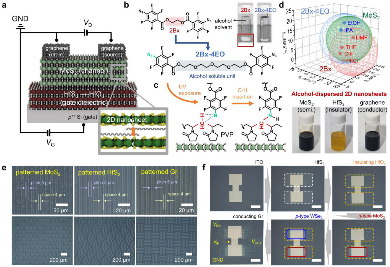 Figure 1. Schematic overview of the fully photopatterned 2D nanomaterial-based FET fabrication process.
A critical aspect of this development was identifying a suitable solvent and cross-linker combination. Through detailed analysis using Hansen solubility parameters, the team selected isopropanol as the solvent, and modified the chemical structure of conventional azide-based cross-linkers to ensure compatibility and stable dispersion of the 2D materials. Notably, azide cross-linkers, typically insoluble in alcohols, were engineered for solubility in isopropanol, enabling effective UV-induced cross-linking.
Using this technique, the team fabricated molybdenum disulfide (MoS₂) transistors exhibiting a charge carrier mobility of 20.2 cm²/V·s, a threshold voltage of 2.0 V, and an on/off ratio of 2.7 million. An array of 49 transistors demonstrated stable operation over more than 60 days without performance degradation. Furthermore, the researchers successfully patterned both p-type and n-type 2D semiconductors on a single substrate to create logic circuits-including NOT, NAND, NOR gates-and static random-access memory (SRAM), demonstrating the method's potential for practical device integration.
Professor Kim commented, "This study extends UV cross-linking technology-originally used in quantum dot displays-to 2D semiconductor materials, marking a significant step toward environmentally friendly, high-precision patterning of sensitive nanoscale devices. We believe this approach will play a crucial role in developing next-generation, energy-efficient, high-speed semiconductor chips."
Supported by Samsung Research Funding & Incubation Center, this research was led by UNIST researcher Wan Ho Cho, with key contributions from In Cheol Kwak and Se-Jin Kim at Yonsei University. The findings are scheduled for publication in Advanced Materials.
Journal Reference
In Cheol Kwak, Se-Jin Kim, Wan Ho Cho, et al., "Direct Photopatterning of Green Solvent-Processed 2D Nanomaterials for Wafer-Scale Electronics," Adv. Mater., (2025).


