What the research is about
When we watch videos or ask AI questions, enormous amounts of data are constantly moving inside computers. In particular, data centers that support AI must process and transfer vast amounts of data at very high speeds. However, current computers have a fundamental limitation: the place where calculations are performed and the place where data is stored are physically separated.
Because of this, data has to travel back and forth many times within a chip. This repeated movement takes time and consumes energy, creating a bottleneck that limits both speed and efficiency.
One promising way to solve this problem is to place memory very close to the computing circuits. This reduces the distance that data needs to travel. Such an approach, where computing and memory are integrated, is known as logic-embedded memory and is being actively studied worldwide.
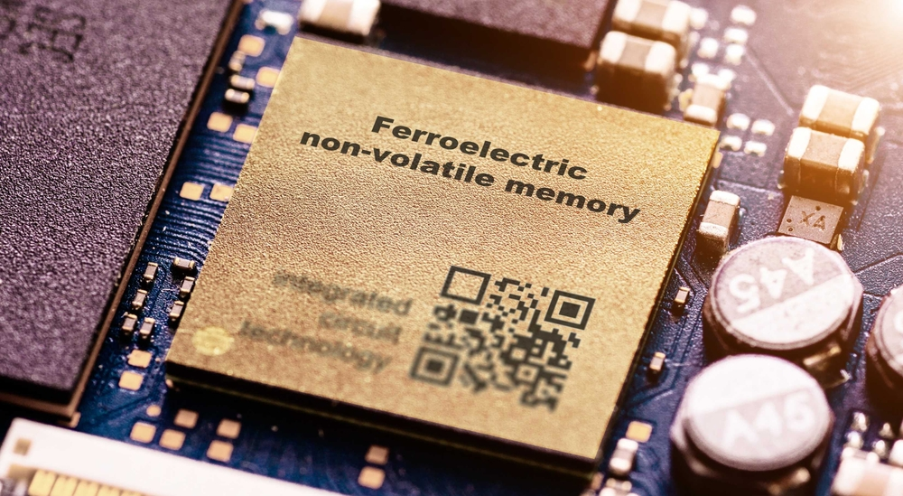
A material attracting attention for this purpose is aluminum scandium nitride. This material can retain information even when the power is turned off and is also resistant to high temperatures during device fabrication.
Previous studies have mainly focused on making thin layers of this material and investigating how thin they can be. However, real memory devices consist of multiple stacked layers, including electrodes. As a result, it has remained unclear how thin the entire device can be made.
To address this challenge, a research team led by Professor Hiroshi Funakubo at Institute of Science Tokyo (Science Tokyo) set out to minimize the thickness of the entire memory device.
Why this matters
The team successfully reduced the total thickness of the memory device to just 30 nanometers, by combining platinum electrodes with a thin film of aluminum scandium nitride. This is about one three-thousandth the thickness of a human hair.
The main challenge was that simply making the device thinner can degrade its performance. When the film becomes too thin, the internal crystal structure can become disordered, weakening its function as a memory device.
To overcome this, the researchers applied heat treatment to the lower electrode before forming the film. This improved the alignment of the crystals in the film, allowing the device to maintain high performance even at a thickness of just 20 nanometers.
They also found that the electrodes themselves could be made as thin as 5 nanometers without degrading performance. These results demonstrate a viable path toward scaling down the entire memory device while maintaining its functionality.
What's next
This research represents an important step toward next-generation semiconductor chips that integrate computing and memory. If such memory devices can be put into practical use, they could significantly reduce data movement, enabling faster operation with much lower energy consumption.
This would benefit a wide range of applications, from AI data centers to everyday IoT devices. In addition, because this technology is compatible with existing semiconductor manufacturing processes, it has strong potential for integration into future high-performance chips.
Comment from the researcher
Until now, it was not well understood how thin the entire device could be made. We carefully tested many conditions, including how to treat the electrodes, and finally demonstrated that high performance can be maintained even at just 30 nanometers. We hope this work will contribute to future computing technologies with dramatically reduced energy consumption.
(Hiroshi Funakubo, Professor, School of Materials and Chemical Technology, Institute of Science Tokyo)