Physicists at the University of Würzburg have determined the quantum dynamics in a two-dimensional layer of boron nitride. Their findings form the basis for future applications in quantum technology.
A key factor for the performance of sensors is the speed at which the system returns to its initial state after a disturbance or measurement, similar to the taring of a balance. In the quantum sensor under investigation, this corresponds to the transition of electrons from an energetically excited state to the ground state. However, the electrons remain in a kind of "metastable intermediate state" for a short time. A team of physicists from Julius-Maximilians-Universität Würzburg (JMU) has now directly measured this "waiting time" in a two-dimensional material: it lasts exactly 24 billionths of a second.
This knowledge is particularly important for quantum technology. It can be used to significantly increase the accuracy of atomic sensors, paving the way for the medical diagnostics of the future, for example. Professor Vladimir Dyakonov, Head of the Chair of Experimental Physics VI (EPVI), was responsible for the study, which has been published in the journal Science Advances .
Defects as the basis of quantum sensors
Background: In modern quantum technology, so-called atomic defects in solids form the basis for precise measuring instruments. For a long time, diamond was considered the standard material for quantum sensors, as its three-dimensional crystal structure effectively protects against external interference. If one of these atoms is missing in the normally perfect lattice of carbon atoms, this defect acts as a tiny quantum sensor whose properties can be controlled using lasers and microwaves.
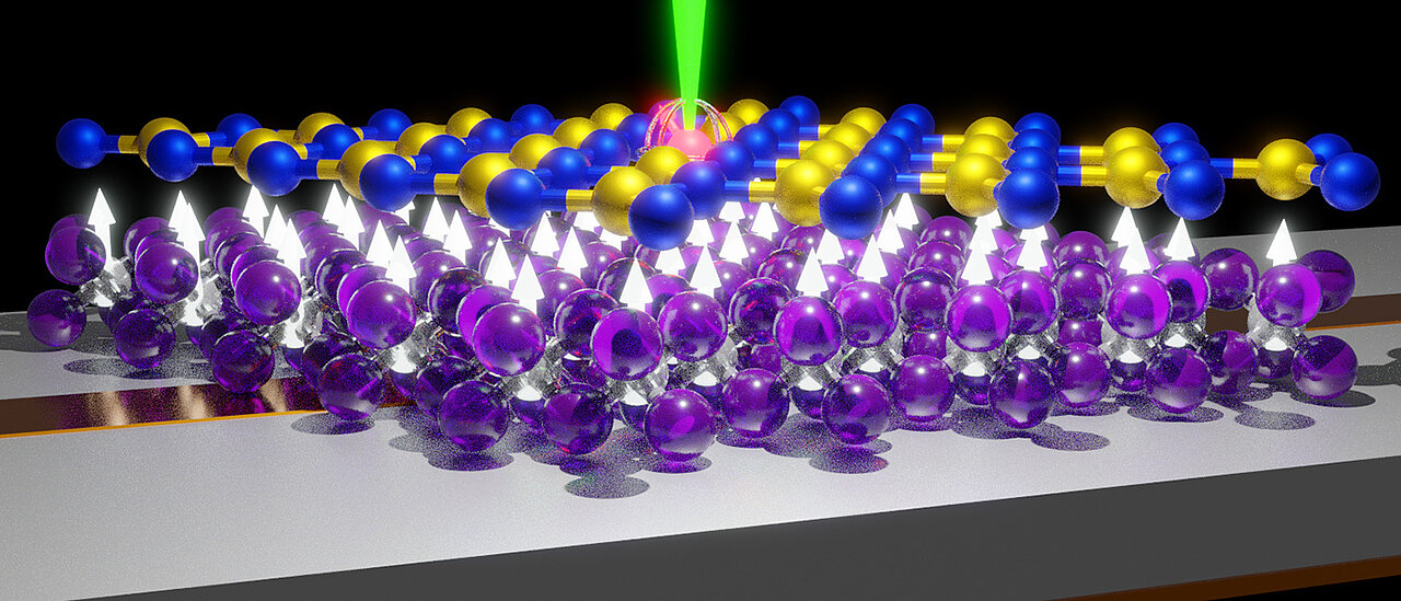
The problem is that in the three-dimensional diamond lattice, the distance between the sensor defect and the object to be analysed is relatively large, which reduces the signal strength. The situation is different with the material that the Würzburg team investigated: hexagonal boron nitride (hBN) - a two-dimensional material made up of a single layer of atoms.
"In contrast to 3D crystals, hBN allows the positioning of spin defects with atomic precision within a very thin layer," says Vladimir Dyakonov, explaining the key advantage of this material. This enables a significantly smaller distance to the measurement object and therefore a stronger interaction. The negatively charged boron defects are particularly promising, as they can also be addressed optically at room temperature. However, to fully utilise the potential of these 2D sensors, mere spatial proximity is not enough; it is imperative to understand the internal "clock" and the dynamic processes of these defects in detail.
Electrons remain in a holding pattern
The speed at which the system returns to its ground state after optical excitation is a decisive factor. A so-called "metastable intermediate state", figuratively speaking a kind of car park or waiting room for electrons, plays an important role here: Before electrons can return to the ground state, they remain in this state for a short time, which limits the sequence of measurement cycles.


