An artistic image of a futuristic semiconductor device which will help make 6G technology a reality.University of Bristol
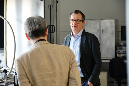
Image shows Professor Martin Kuball at the Centre for Device Thermography and Reliability (CDTR), based at the University of Bristol, which unites scientists from across the world to develop next generation semiconductor electronic devices.University of Bristol
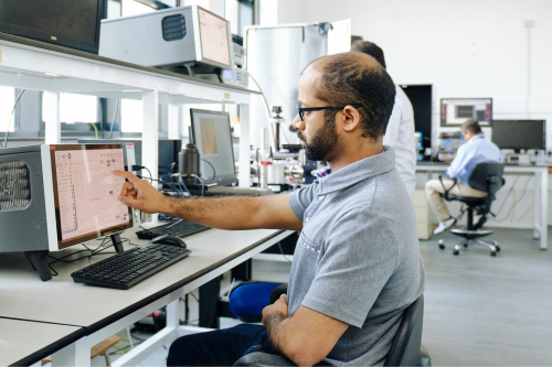
Image shows Dr Akhil Shaji at work in the Centre for Device Thermography and Reliability (CDTR).University of Bristol
Self-driving cars which eliminate traffic jams, getting a healthcare diagnosis instantly without leaving your home, or feeling the touch of loved ones based across the continent may sound like the stuff of science fiction.
But new research, led by the University of Bristol and published today in the journal Nature Electronics, could make all this and more a step closer to reality thanks to a radical breakthrough in semiconductor technology.
The futuristic concepts rely on the ability to communicate and transfer vast volumes of data much faster than existing networks. So physicists have developed an innovative way to accelerate this process between scores of users, potentially across the globe.
Co-lead author Martin Kuball, Professor of Physics at the University of Bristol, said: "Within the next decade, previously almost unimaginable technologies to transform a wide range of human experiences could be widely available. The possible benefits are also far-reaching, including advances in healthcare with remote diagnostics and surgery, virtual classrooms and even virtual holiday tourism.
"In addition, there is considerable potential for advanced driver assistance systems to improve road safety and industrial automation for greater efficiency. The list of possible 6G applications is endless, with the limit just being human imagination. So our innovative semiconductor discoveries are hugely exciting and will help drive forward these developments at speed and scale."
It is widely acknowledged that the shift from 5G to 6G will demand a radical upgrade of semiconductor technology, circuits, systems, and associated algorithms. For instance, the main semiconductor components involved, in other words the radio frequency amplifiers made from a wonder conductor called Gallium Nitride (GaN), need to be much quicker, emit greater power, and be more reliable.
The team of international scientists and engineers has tested a new architecture, catapulting these special GaN amplifiers to unprecedented heights. This was achieved by discovering a latch-effect in GaN, which unlocked a much greater radio frequency device performance. These next generation devices use parallel channels which then require the use of sub-100nm side fins – a type of transistor which controls the flow of current passing through the devices.
Co-lead author Dr Akhil Shaji, Honorary Research Associate at the University of Bristol, explained: "We have piloted a device technology, working with collaborators, called superlattice castellated field effect transistors (SLCFETs), in which more than 1000 fins with sub-100 nm width help drive the current. Although SLCFETs have demonstrated the highest performance in the W-band frequency range, equating to 75 gigahertz -110 GHz, the physics behind it was unknown.
"We recognised it was a latch-effect in GaN, which enables the high radio frequency performance."
The researchers then needed to pinpoint exactly where this effect occurred, by simultaneously using ultra precision electrical measurements and optical microscopy, so it could be further studied and understood. After analysing more than 1,000 fins findings located this effect to the widest fin.
Prof Kuball, who is also Royal Academy of Engineering Chair in Emerging Technologies, added: "We also developed a 3D model using a simulator to further verify our observations. The next challenge was to study the reliability aspects of latch effect for practical applications. The rigorous testing of the device over a long duration of time showed it has no detrimental effect on device reliability or performance.
"We found a key aspect driving this reliability was a thin layer of dielectric coating around each of the fins. But the main takeaway was clear – the latch effect can be exploited for countless practical applications, which could help transform people's lives in many different ways in years to come."
Next steps for the work include further increasing the power density the devices can deliver, so they can offer even higher performance and serve wider audiences. Industry partners will also be bringing such next generation devices to a commercial market.
Researchers at the University of Bristol are at the forefront of improving electrical performance and efficiency in a wide range of different applications and settings.
Professor Kuball leads the Centre for Device Thermography and Reliability (CDTR), which is developing next generation semiconductor electronic devices for net zero, and for communications and radar technology. It also works on improving device thermal management, electrical performance and reliability, using wide and ultra-wide bandgap semiconductors.
Paper
'Gallium nitride multichannel devices with latch-induced sub-60-mV-per-decade subthreshold slopes for radiofrequency applications' by A.S Kumar et al in Nature Electronics