A NASA-sponsored team is advancing single-photon sensing Complementary Metal-Oxide-Semiconductor (CMOS) detector technology that will enable future NASA astrophysics space missions to search for life on other planets. As part of their detector maturation program, the team is characterizing sensors before, during, and after high-energy radiation exposure; developing novel readout modes to mitigate radiation-induced damage; and simulating a near-infrared CMOS pixel prototype capable of detecting individual photons.
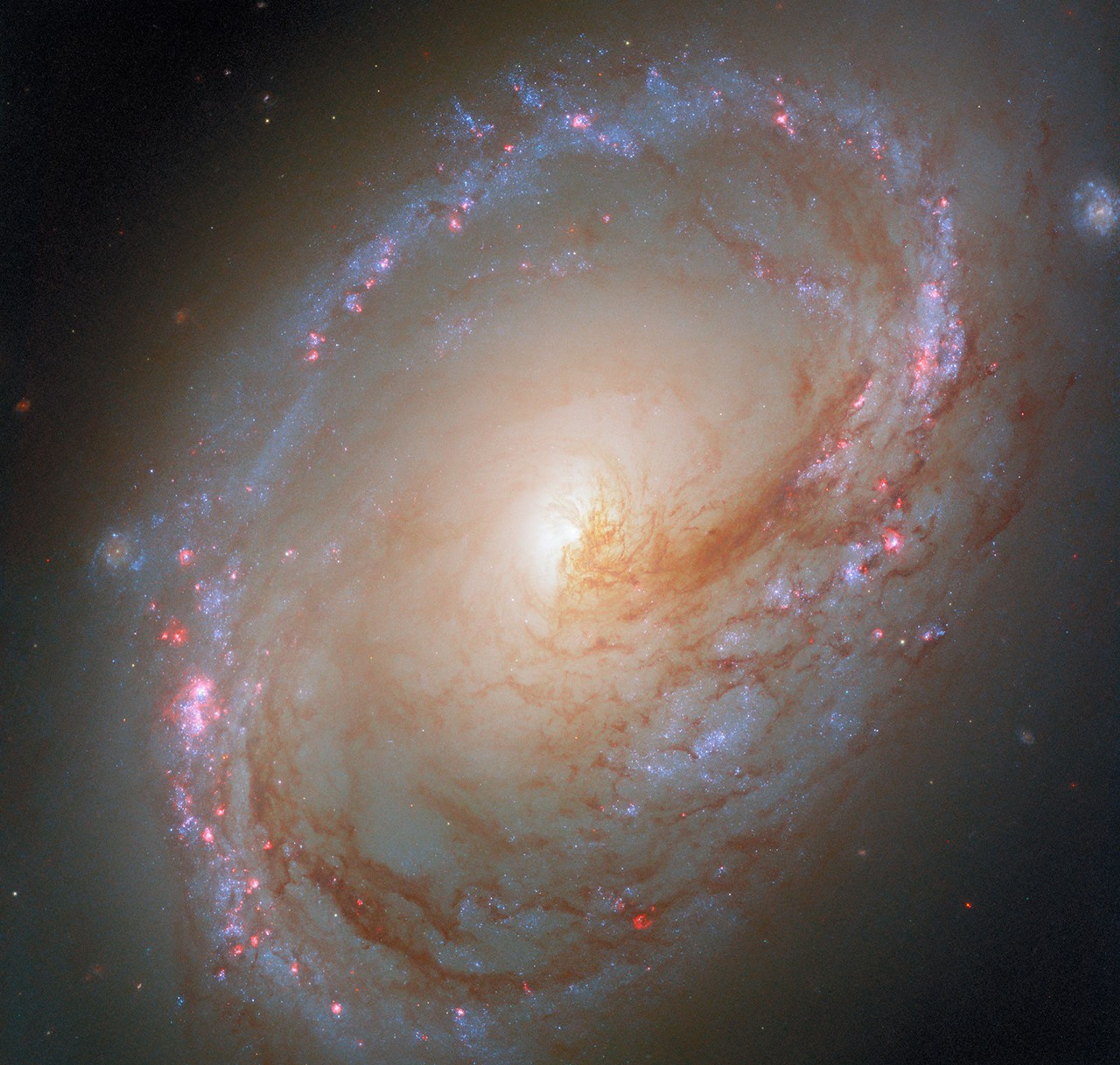
Are we alone in the universe? This age-old question has inspired scientific exploration for centuries. If life on other planets evolves similarly to life on Earth, it can imprint its presence in atmospheric spectral features known asbiosignatures. They include absorption and emission lines in the spectrum produced by oxygen, carbon dioxide, methane, and other molecules that could indicate conditions which can support life. A future NASA astrophysics mission, the Habitable Worlds Observatory (HWO), will seek to find biosignatures in the ultraviolet, optical, and near-infrared (NIR) spectra of exoplanet atmospheres to look for evidence that life may exist elsewhere in the universe.
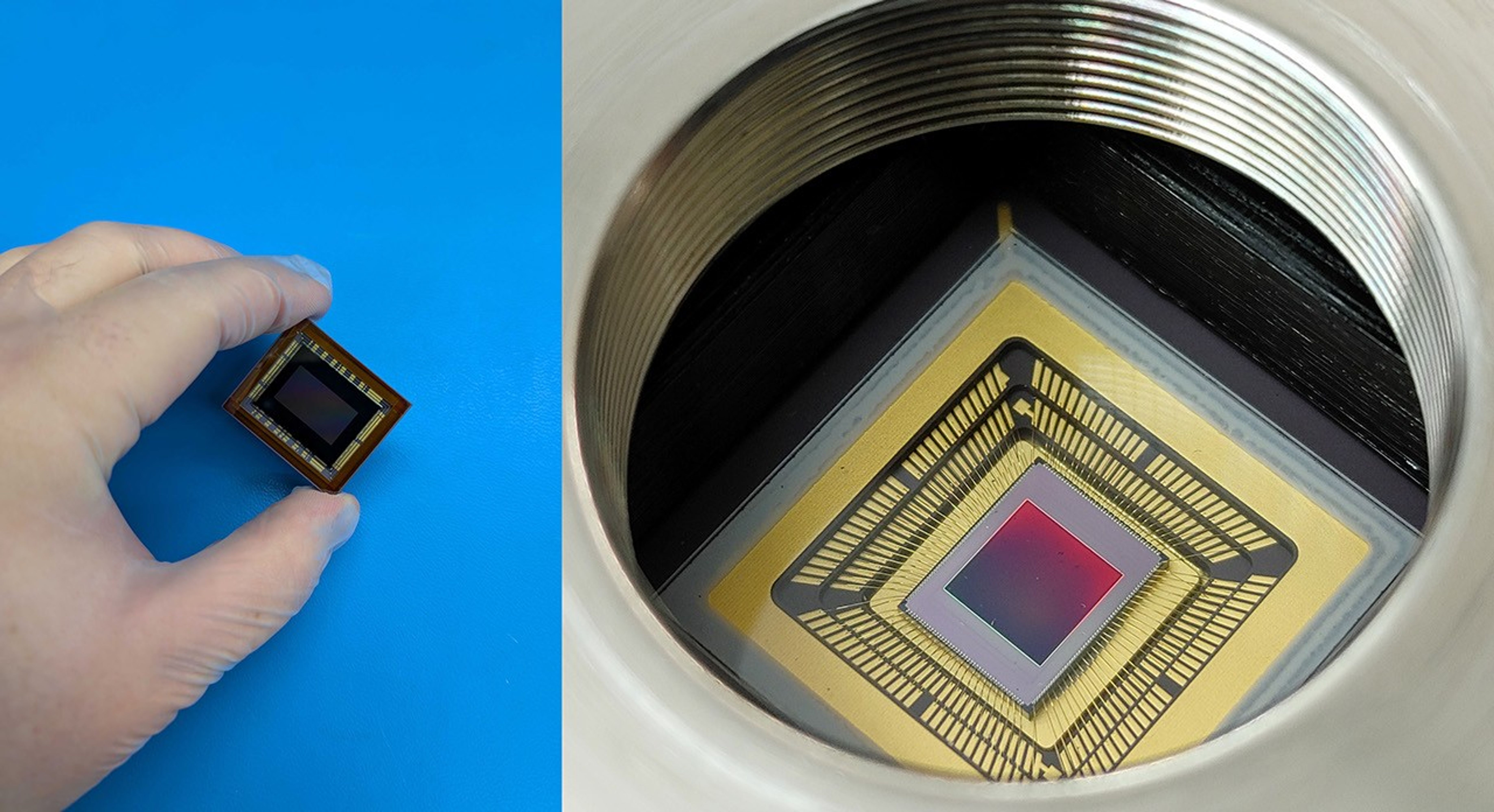
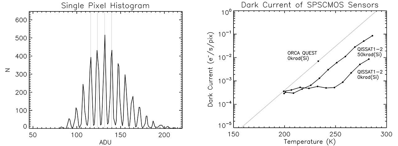
HWO will need highly sensitive detector technology to detect these faint biosignatures on distant exoplanets. The Single-Photon Sensing Complementary Metal-Oxide-Semiconductor (SPSCMOS) image sensor is a promising technology for this application. These silicon-based sensors can detect and resolve individual optical-wavelength photons using a low-capacitance, high-gain floating diffusion sense node. They operate effectively over a broad temperature range, including at room temperature. They have near-zero read noise, are tolerant to radiation, and generate very little unwanted signal-such as dark current. When cooled to 250 K, the dark current drops to just one electron every half-hour. If either the read noise or dark current is too high, the sensor will fail to detect the faint signals that biosignatures produce.
A research team at the Rochester Institute of Technology (RIT) Center for Detectors (CfD) is accelerating the readiness of these SPSCMOS sensors for use in space missions through detector technology maturation programs funded by NASA's Strategic Astrophysics Technology and Early Stage Innovations solicitations. These development programs include several key goals:
- Characterize critical detector performance metrics like dark current, quantum efficiency, and read noise before, during, and after exposure to high-energy radiation
- Develop new readout modes for these sensors to mitigate effects from short-term and long-term radiation damage
- Design a new NIR version of the sensor using Technology Computer-Aided Design (TCAD) software
SPSCMOS sensors operate similarly to traditional CMOS image sensors but are optimized to detect individual photons-an essential capability for ultra-sensitive space-based observations, such as measuring the gases in the atmospheres of exoplanets. Incoming photons enter the sensor and generate free charges (electrons) in the sensor material. These charges collect in a pixel's storage well and eventually transfer to a low-capacitance component called the floating diffusion (FD) sense node where each free charge causes a large and resolved voltage shift. This voltage shift is then digitized to read the signal.
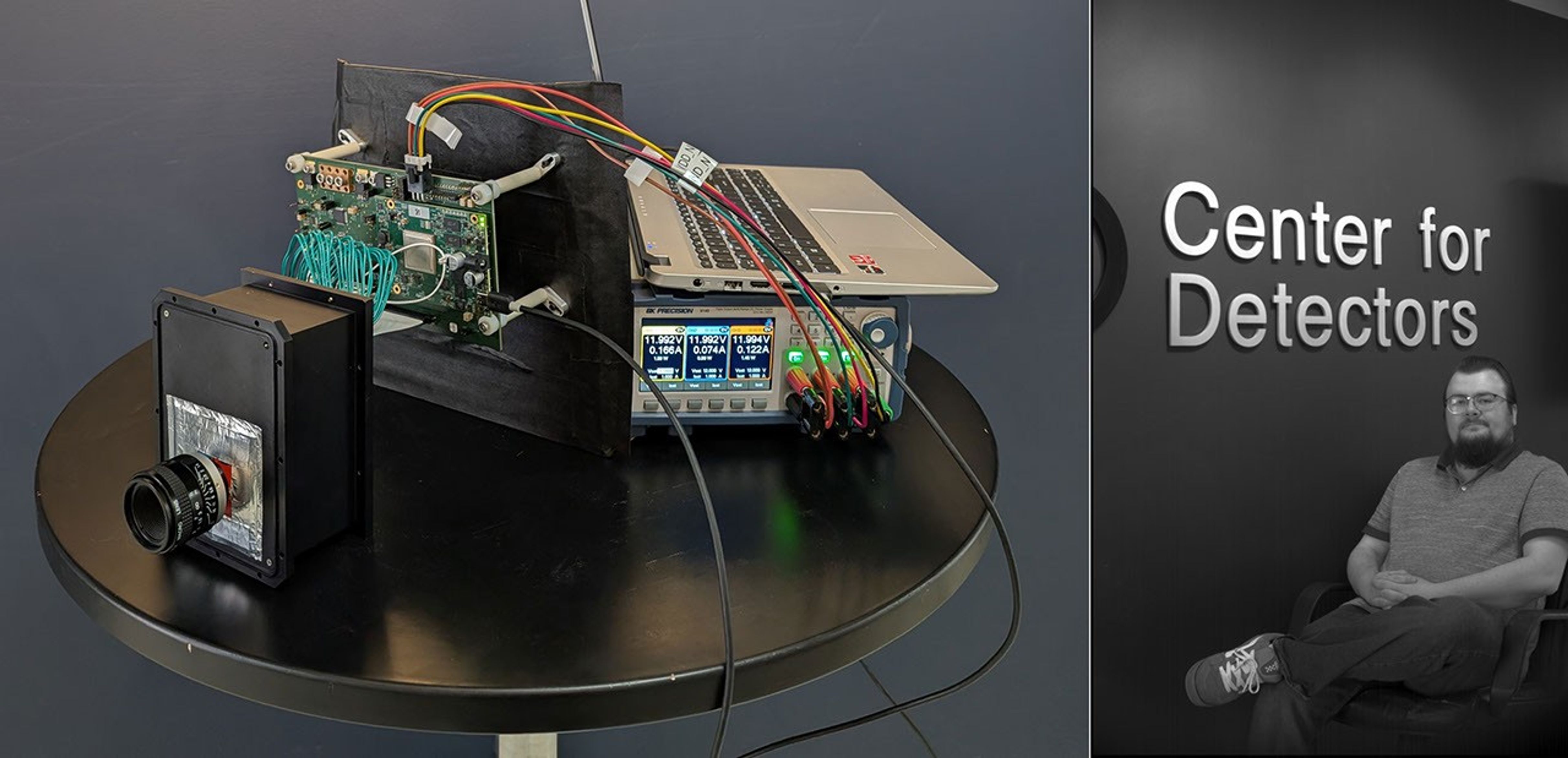
Experiments that measure sensor performance in a space relevant environment use a vacuum Dewar and a thermally-controlled mount to allow precise tuning of the sensors temperature. The Dewar enables testing at conditions that match the expected thermal environment of the HWO instrument, and can even cool the sensor and its on-chip circuits to temperatures colder than any prior testing reported for this detector family. These tests are critical for revealing performance limitations with respect to detector metrics like dark current, quantum efficiency, and read noise. As temperatures change, the electrical properties of on-chip circuits can also change, which affects the read out of charge in a pixel.
The radiation-rich environment for HWO will cause temporary and permanent effects in the sensor. These effects can corrupt the signal measured in a pixel, interrupt sensor clocking and digital logic, and can cause cumulative damage that gradually degrades sensor performance. To mitigate the loss of detector sensitivity throughout a mission lifetime, the RIT team is developing new readout modes that are not available in commercial CMOS sensors. These custom modes sample the signal over time (a "ramp" acquisition) to enable the detection and removal of cosmic ray artifacts. In one mode, when the system identifies an artifact, it segments the signal ramp and selectively averages the segments to reconstruct the original signal-preserving scientific data that would otherwise be lost. In addition, a real-time data acquisition system monitors the detector's power consumption, which may change from the accumulation of damage throughout a mission. The acquisition system records these shifts and communicates with the detector electronics to adjust voltages and maintain nominal operation. These radiation damage mitigation strategies will be evaluated during a number of test programs at ground-based radiation facilities. The tests will help identify unique failure mechanisms that impact SPSCMOS technology when it is exposed to radiation equivalent to the dose expected for HWO.
While existing SPSCMOS sensors are limited to detecting visible light due to their silicon-based design, the RIT team is developing the world's first NIR single-photon photodiode based on the architecture used in the optical sensors. The photodiode design starts as a simulation in TCAD software to model the optical and electrical properties of the low-capacitance CMOS architecture. The model simulates light-sensitive circuits using both silicon and Mercury Cadmium Telluride (HgCdTe or MCT) material to determine how well the pixel would measure photo-generated charge if a semiconductor foundry physically fabricated it. It has 2D and 3D device structures that convert light into electrical charge, and circuits to control charge transfer and signal readout with virtual probes that can measure current flow and electric potential. These simulations help to evaluate the key mechanisms like the conversion of light into electrons, storing and transferring the electrons, and the output voltage of the photodiode sampling circuit.
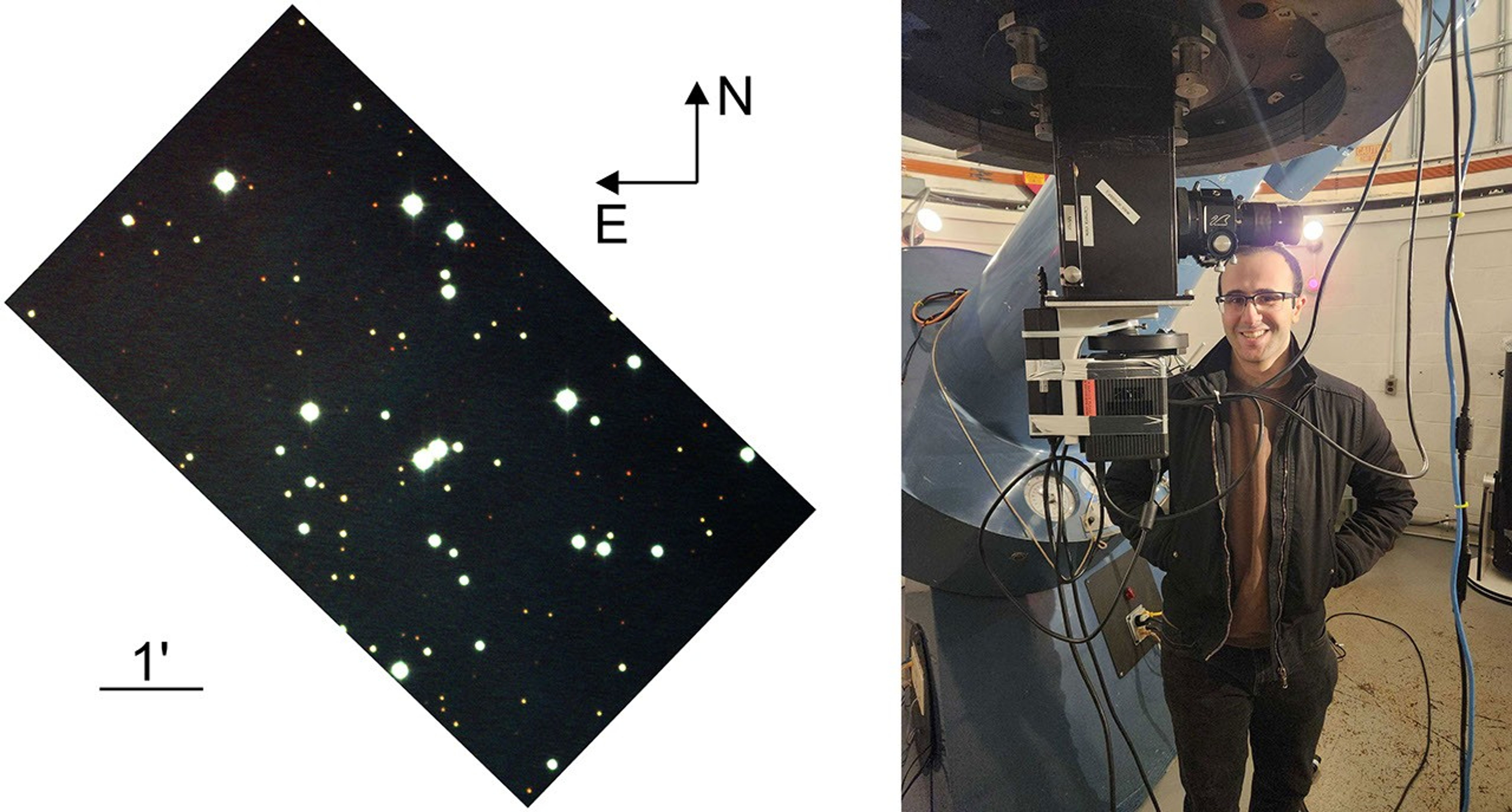
In addition to laboratory testing, the project includes performance evaluations at a ground-based telescope. These tests allow the sensor to observe astronomical targets that cannot be fully replicated in lab. Star fields and diffuse nebulae challenge the detector's full signal chain under real sky backgrounds with faint flux levels, field-dependent aberrations, and varying seeing conditions. These observations help identify performance limitations that may not be apparent in controlled laboratory measurements.
In January 2025, a team of researchers led by PhD student Edwin Alexani used an SPSCMOS-based camera at the C.E.K. Mees Observatory in Ontario County, New York. They observed star cluster M36 to evaluate the sensor's photometric precision, and the Bubble Nebula in a narrow-band H-alpha filter. The measured dark current and read noise were consistent with laboratory results.
The team observed photometric reference stars to estimate the quantum efficiency (QE) or the ability for the detector to convert photons into signal. The calculated QE agreed with laboratory measurements, despite differences in calibration methods.
The team also observed the satellite STARLINK-32727 as it passed through the telescope's field of view and measured negligible persistent charge-residual signal that can remain in detector pixels after exposure to a bright source. Although the satellite briefly produced a bright streak across several pixels due to reflected sunlight, the average latent charge in affected pixels was only 0.03 e-/pix - well below both the sky-background and sensor's read noise.
As NASA advances and matures the HWO mission, SPSCMOS technology promises to be a game-changer for exoplanet and general astrophysics research. These sensors will enhance our ability to detect and analyze distant worlds, bringing us one step closer to answering one of humanity's most profound questions: are we alone?
For additional details, see the entry for this project on NASA TechPort.
Project Lead(s): Dr. Donald F. Figer, Future Photon Initiative and Center for Detectors, Rochester Institute of Technology (RIT), supported by engineer Justin Gallagher and a team of students.
Sponsoring Organization(s): NASA Astrophysics Division, Strategic Astrophysics Technology (SAT) Program and NASA Space Technology Mission Directorate (STMD), Early Stage Innovations (ESI) Program