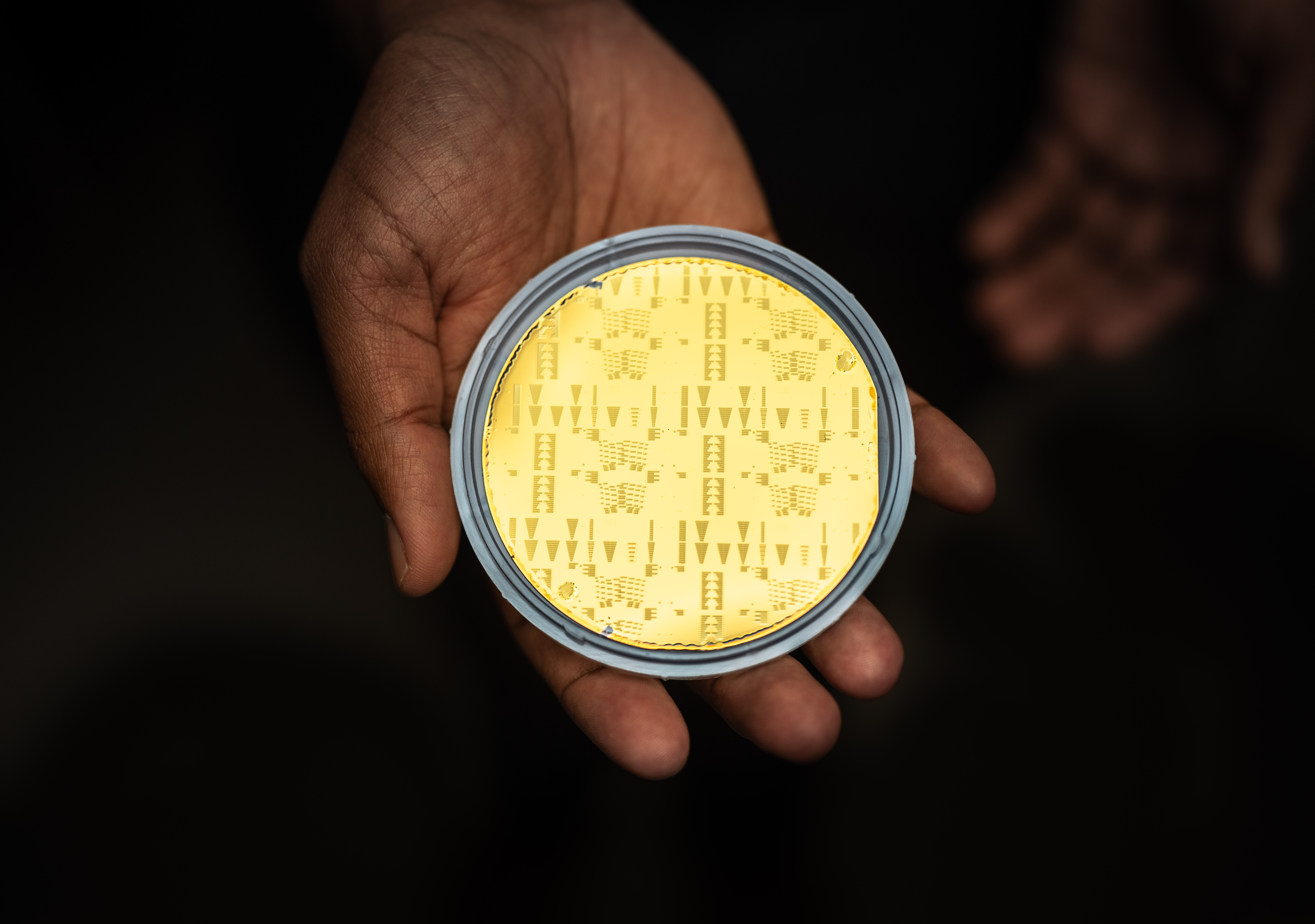
More than a thousand experimental lasers and amplifiers adorn a three-inch, gold-electroplated silicon wafer made at Sandia National Laboratories' Microsystems Engineering, Science and Applications complex. (Photo by Craig Fritz) Click on the thumbnail for a high-resolution image.
The laser is so small you need a microscope to see it properly. But it's not just the size that scientists at Sandia National Laboratories are excited about.
The buzz is that the laser can now be combined with other microscale optical devices to make self-driving cars safer, data centers more efficient, biochemical sensors more portable and radars and other defense technologies more versatile.
Sandia has been awarded a patent for its new method of integrating many different materials onto silicon - the same starting material semiconductor fabrication plants use to make microchips.
This method enables Sandia to build high-bandwidth, high-speed optical devices, including indium phosphide lasers, lithium niobate modulators, germanium detectors and low-loss acousto-optic isolators - all critical components for high-power optical systems.


