
In Brief
- A team led by WashU's Rohan Mishra has shown how atomic-scale control of oxides compatible with chip manufacturing can yield next-generation innovations for memory and energy storage.
- Mishra and team combined quantum-mechanical modeling and atomic-resolution electron microscopy with materials synthesis by collaborators at multiple institutions to make these discoveries.
The growth of artificial intelligence has increased demand for more efficient data storage. Instead of adding bulk to satiate this appetite, researchers at Washington University in St. Louis are working to increase memory capacity by manipulating materials' characteristics at the atomic level.
Rohan Mishra, an associate professor of mechanical engineering and materials science at the McKelvey School of Engineering, and his team of researchers have been pursuing this challenge with funding from the National Science Foundation. Through computational modeling, advanced microscopy and experimental collaboration with researchers at the University of Nebraska-Lincoln, Georgia Institute of Technology (Georgia Tech) and other institutions, Mishra and his team have made exciting insights into material behavior.
Making materials used for silicon-based transistors work
One of Mishra's research areas focuses on hafnia (HfO2), which makes up the thin, insulating layer in silicon-based transistors.
If the material were ferroelectric, it would maintain an electrical polarization that can reverse direction when an electric field is applied. More important, the material would remember which direction its polarization points, even after the electric field is removed. This feature would make hafnia a good candidate for memory storage.
The problem is that most materials lose their ferroelectric behavior when they are extremely thin (less than 10 nanometers; for reference, a human hair is about 80,000 nanometers wide). But a group of researchers in Germany found that hafnia does not. They showed that extremely thin hafnia demonstrates ferroelectric behavior.
It was head-scratching behavior: Hafnia, a material otherwise not ferroelectric, suddenly becomes ferroelectric when extremely thin.

"It was a puzzle we are trying to understand," Mishra says. His solution to that puzzle was published in Science. As part of the investigation, Mishra collaborated with the team of Xiaoshan Xu at the University of Nebraska-Lincoln to grow well-ordered, single-crystal films of lanthanum-doped hafnia on a substrate.
Guodong Ren, who completed his doctoral degree under Mishra's supervision and now works as a postdoctoral researcher at the University of Washington, confirmed the single crystalline structure of the thin hafnia films using advanced microscopy to resolve individual atomic columns in materials.
The researchers then determined the phase and behavior of the single crystals using electron microscopy. The results lined up with the predictions from their computational models.
The takeaway, according to Mishra, is that instead of struggling to force hafnia into a conventional ferroelectric phase, engineers might stabilize it more favorably with antiferroelectric structure in thin films and then control the transition electrically.
"Instead of fighting nature, we can grow high-quality antiferroelectric films and we can then switch them during operation," Mishra said. Another advantage of antiferroelectrics, he said, is that they store a lot of energy and can be used as high-energy density capacitors.
The intersection between modeling, microscopy and experimentation
The researchers in Mishra's group complement atomic scale modeling - studying the stability and properties of an ensemble of atoms - with microscopy observations of synthesized materials.
"When you synthesize real materials, they always have defects, so our work was to understand how to minimize these defects so we can grow a high-quality film," Mishra said.
The group used quantum mechanics to model and predict material behavior from the atomic scale up, then collaborated with external groups to synthesize materials that closely align with the models. Once they were synthesized, Ren evaluated what the real materials looked like at the atomic level.
"Guodong is an expert in combining theory and microscopy, one of the very few people who can do it at that level," Mishra said.
"Microscopy is a two-dimensional projection of a three-dimensional structure, so it helps us retrieve the real structure of the materials we study using a combination of microscopy and quantum mechanical calculations," he said.
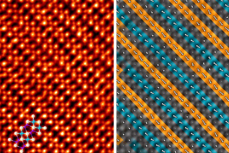
Ren is also a co-first author of a separate study, co-led by Mishra and Asif Khan at Georgia Tech and Jun Hee Lee at UNIST, South Korea, and published in Advanced Materials — which observed extremely small ferroelectric domains in zirconia (ZrO2, a close analogue of hafnia) with footprints of less than one square nanometer. The researchers found that within each domain, electrical polarization points in a particular direction. Extra oxygen atoms helped balance electrical charge on the boundaries between these domains. Here, too, their calculations predicted that the domain walls could conduct electricity and move in response to an electric bias, which suggested that such atomically thin walls could one day serve as electronic components for memory storage.
Ren appreciates the holistic approach to exploring ferroelectric materials in the Mishra group. "We have a unique chance to combine theoretical studies and also microscopy experiments at the atomic level so we can gain a better understanding about different material systems," Ren said.
The studies together present the idea of engineers controlling electronic behavior by manipulating materials at the atomic level. Even better, according to Mishra and Ren, some of these materials are in the silicon chips we already use, so manufacturers need not add new components.
N. Afroze, H. Fahrvandi, G. Ren, et al. " Sub-nm2 Ferroelectric Domains via Charged 180° Walls in ZrO2." Advanced Materials (2026): e75144. DOI: https://10.1002/adma.75144
Xin Li et al. Antiferroelectric hafnia down to the 2D limit. Science (24 Sep 2026), eady5526 DOI:10.1126/science.ady5526
Work at WashU was supported by NSF awards DMR-214579 and DMR-2122070.
Originally published on the McKelvey Engineering website


