Key Takeaways
- Berkeley Lab scientists developed a new way to determine atomic structures from nanocrystals previously considered unusable for crystallography.
- By combining 4D-STEM with computational "virtual apertures," the team can isolate and analyze individual nanocrystals embedded within dense clusters - without requiring large, pristine samples.
- The results represent the first single-crystal structures determined from 4D-STEM data by direct methods at subangstrom resolution.
Scientists at the Department of Energy's Lawrence Berkeley National Laboratory (Berkeley Lab) have developed a new way to determine atomic structures from nanocrystals previously considered unusable, a breakthrough that could transform how researchers study materials too small or imperfect for conventional crystallography.
Crystalline materials have enabled advances in computing, communications, energy technologies, and pharmaceuticals. Many of these materials' unique properties arise from the way in which their constituent molecules form repeating patterns. To better understand how to develop crystalline materials into useful technologies, scientists need to determine their atomic structure. Unfortunately, their samples don't always cooperate. Although established techniques like X-ray crystallography can deliver beautiful maps of atomic structure at subangstrom resolution, they require large, pristine single crystals to work, and many important materials refuse to grow that way.
Now, in a recent study published in the Proceedings of the National Academy of Sciences (PNAS), Berkeley Lab scientists have developed an approach that can sample single nanocrystals embedded within agglomerated clusters, transforming once-problematic materials into valuable sources of data.
"Our technique allows us to selectively mine data from the best areas of a nanoscale sample, which is a game changer for crystallography," said senior author Peter Ercius, staff scientist at the Molecular Foundry's National Center for Electron Microscopy (NCEM) facility.
Using a technique called 4D-STEM (four-dimensional scanning transmission electron microscopy), the Berkeley Lab researchers shrink the electron beam down to just a few nanometers and raster-scan it across their sample in small, precise steps. At each of the hundreds of thousands of probe positions in their experiment, they record an independent diffraction pattern, building up a massive dataset.
"Our technique allows us to selectively mine data from the best areas of a nanoscale sample, which is a game changer for crystallography." - Peter Ercius, staff scientist at the Molecular Foundry's National Center for Electron Microscopy (NCEM) facility
The achievement advances the use of electron microscopes in crystallography. Recently, crystallographers have turned to a technique called microcrystal electron diffraction (MicroED) to analyze nanoscale samples. Since high-energy electrons interact with matter more strongly than X-rays, they allow scientists to image nanocrystals even smaller than the wavelength of visible light. Using electrons, researchers can now solve atomic structures from specimens previously considered too small to be usable.
Yet even MicroED has its limitations, according to first author Ambarneil Saha, postdoctoral fellow at NCEM. MicroED bathes everything in its path with a broad electron beam, typically a few micrometers wide. Then, researchers insert an aperture inside the microscope to try and isolate the signal from the target crystal. If multiple crystals clump together within the area covered by the aperture, their diffraction patterns also blur together, producing difficult-to-interpret results.
The team's custom-built detector, the 4D Camera, helped them overcome such limitations. Operating at a lightning-fast 87,000 frames per second, the 4D Camera - installed on the TEAM 0.5 microscope at NCEM - produces a bitrate around 1500 times faster than the average internet download speed in the U.S. This torrent of data is then streamed to the Perlmutter supercomputer at Berkeley Lab's National Energy Research Scientific Computing Center (NERSC), where dedicated algorithms compress and process it in real time.
"Our approach brings together expertise in detector engineering, supercomputing, electron microscopy, and crystallography," said Ercius. "To handle the deluge of data produced by our camera, we used Perlmutter to compress terabytes of sparse frames. We then figured out how to adapt programs from X-ray crystallography to process electron microscopy data from a unique new detector."
Mining data from MOFs
To demonstrate their method, the team worked with the model compound UiO-66, a metal-organic framework (MOF) that forms porous octahedral crystals roughly 300 nanometers wide. While this material had previously been characterized using X-rays, getting clean diffraction data required painstakingly growing much larger crystals.
The key breakthrough came from what the team calls "virtual apertures"- a computational technique that lets them choose which parts of their sample to analyze. They can isolate individual nanocrystals within a conglomerate of nanocrystals, or even pinpoint the specific subregions within a single nanocrystal that produce the best data. Unlike physical apertures whose size and shape are fixed, these virtual apertures can be carefully drawn and optimized into whatever custom shape the researchers need to target atomic regions within a sample.
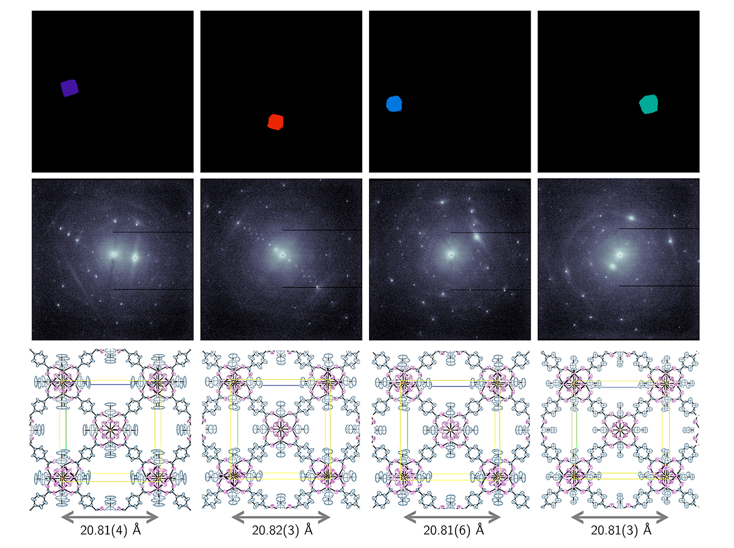
"Nanoscale virtual apertures give us the power to selectively pick the best parts and discard the defective parts, pixel by pixel," explained Saha. "As a crystallographer, that's a dream come true. Not only can we salvage specimens intractable with standard physical apertures, but we can also solve atomic structures from tiny, handpicked subregions within those specimens."
MOFs have been the focus of intense research for next-generation energy, health, and environmental technologies, culminating in the 2025 Nobel Prize in Chemistry shared by Berkeley Lab affiliate Omar Yaghi for their development, work that relied in part on crystallographic studies carried out at Berkeley Lab's Advanced Light Source.
The granular precision of Ercius and Saha's technique could prove transformative across many fields, they said. For example, the technique could help characterize porous MOFs designed for drug delivery or gas capture, providing new insights into how these tiny crystals capture, hold, and release cargo molecules.
"Ultimately, we'd like to develop 4D-STEM into a technique capable of solving single-crystal structures at even smaller length scales," Saha added. "Now we can realistically start targeting populations of unit cells historically inaccessible to crystallography altogether, which is exciting."
The Molecular Foundry and NERSC are DOE Office of Science user facilities at Berkeley Lab.
This work was supported by the DOE Office of Science and Berkeley Lab's Laboratory Directed Research and Development (LDRD) program.