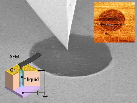
Background micrograph shows an atomic force microscope tip on the surface of a graphene membrane (Gr) covering a liquid-filled channel. (Typical tip radius is tens of nanometers.) Diagram at lower left illustrates how a layer of graphene one atom thick is inserted between the tip and the liquid of interest, which forms an electrical double layer (EDL) on graphene. The graphene barrier prevents a second, unwanted EDL from forming on the tip but still allows the measuring device to map the variation in voltage across the surface of the EDL at high resolution. Micrograph at upper right shows the measured voltage variations across the surface.
Researchers at NIST have devised a way to eliminate a long-standing problem affecting our understanding of both living cells and batteries.
When a solid and an electrically-conducting liquid come into contact, a thin sheet of charge forms between them. Although this interface, known as the electrical double layer (EDL), is only a few atoms thick, it plays a central role in a wide range of systems, such as keeping living cells nourished and maintaining the operation of batteries, fuel cells, and certain types of capacitors.
For instance, the buildup of an EDL on a cell membrane creates a difference in voltage between the liquid environs outside the cell and the cell's interior. The voltage difference draws ions such as potassium from the liquid into the cell, a process essential for the cell's survival and ability to transmit electrical signals.
Within a battery, the EDL that forms between a solid electrode and the electrolyte solution the electrode is immersed in governs the electrochemical reactions that allow charge to flow through the system.
Detailed maps that show exactly how charge is distributed across a surface covered by an EDL could lead to a better understanding of cell function and improve battery life, but the few methods currently available to study this layer lack the ultra-fine spatial resolution to capture such information.
A more promising technique, using the electrically conducting tip of an atomic force microscope (AFM), could--in theory--produce an EDL map resolving features as small as several atoms wide. However, when the tip is immersed in a liquid with a concentration of ions high enough to match that found in batteries or outside living cells, a problem occurs. A second, unwanted EDL forms on the conducting tip, confounding measurements of the EDL that scientists actually want to measure.
"You have two electrical double layers interacting with each other, interfering with the EDL you want to measure and you end up not measuring anything, " said NIST and UMD researcher Evgheni Strelcov.
Strelcov and his colleagues have now circumvented that difficulty, for the first time allowing researchers to map variations in voltage across a sheet of EDL with nanoscale precision. (Voltage measurements indicate the distribution of EDL charge along the surface.) To prevent the spurious EDL from forming, the researchers inserted a barrier--a thin membrane of graphene-between the probe's tip and the liquid.
With the tip no longer in direct contact with the liquid, a sheet of charge could no longer be deposited on the tip and interfere with the measurements. In addition, unlike ordinary metals, graphene is relatively transparent to the electric field associated with the EDL of interest, allowing it to pass through the membrane. That enabled the AFM tip to map variations in the EDL voltage.
Strelcov and his colleagues, including team leader Andrei Kolmakov of NIST and collaborators from the University of Aveiro in Portugal and Oak Ridge National Laboratory, described their findings in the Jan. 28 Nano Letters (https://pubs.acs.org/doi/abs/10.1021/acs.nanolett.9b04823).The team used a laboratory model of an electrolyte solution found in batteries to demonstrate their graphene technique.
EDL's electric charge isn't distributed uniformly across the surface and the high-resolution maps can reveal surface regions where charges clump together. Unevenness in charge distribution along the surface creates hotspots, where electrochemical processes proceed faster.
"The EDL distribution across the surface is complex and since it controls the electrochemical reactions in batteries and biological systems, we must understand it thoroughly to improve the applications' performance," said Strelcov.
Paper: Evgheni Strelcov, Christopher Arble, Hongxuan Guo, Brian D. Hoskins, Alexander Yulaev, Ivan V. Vlassiouk, Nikolai B. Zhitenev, Alexander Tselev and Andrei Kolmakov. Nanoscale Mapping of the Double Layer Potential at the Graphene-Electrolyte Interface. Nano Lett. 2020, 20, 2, 1336-1344, January 28, 2020. https://doi.org/10.1021/acs.nanolett.9b04823


