A research team, led by Professor Hyesung Park in the Deparment of Materials Science and Engineering at UNIST has announced that they have successfully synthesized high-quality large-area monolayer molybdenum diselenide (MoSe2) with good uniformity via promoter-assisted liquid-phase CVD process using the transition metal-containing precursor homogeneously modified with an alkali metal halide.
Carried out in collaboration with Professor Joohoon Kang and his research team from Sungkyunkwan University (SKKU), their findings are expected to help accelerate the commercialization of next-generation semiconductor materials.
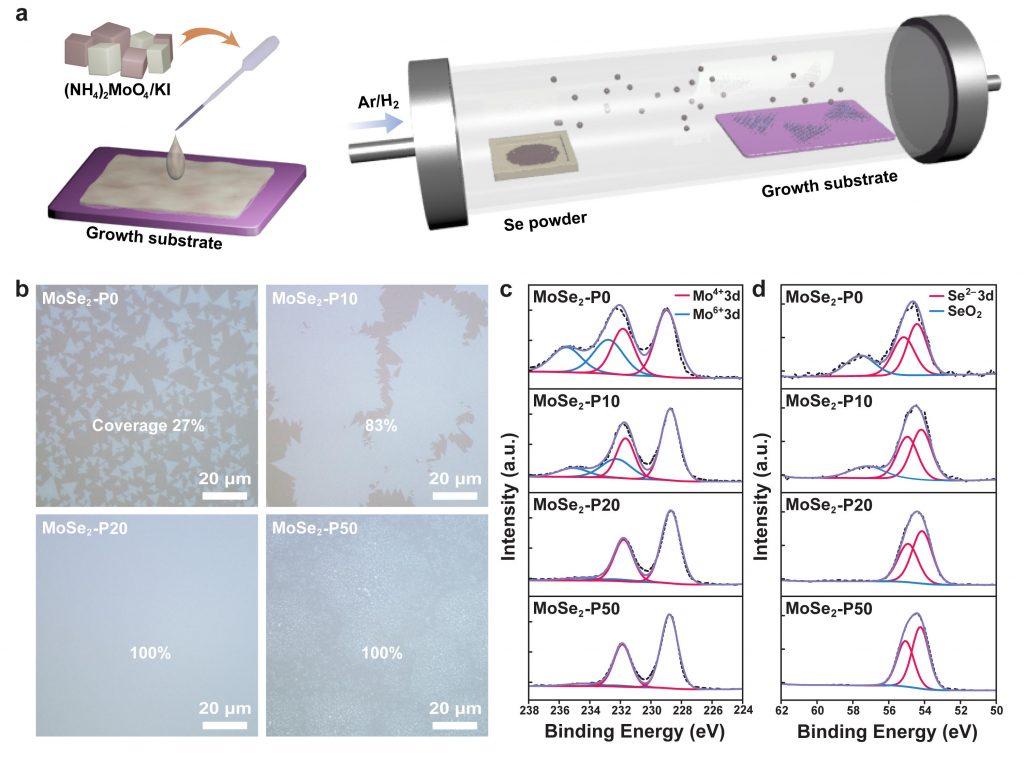
Figure 1. Synthesis of MoSe2 via promoter-assisted liquid-phase CVD. (a) Schematic of the synthesis process for MoSe2 using liquid-phase precursors. (b) OM images of MoSe2 synthesized at different concentrations of potassium iodide. The coverage of the MoSe2 on the growth substrate (sapphire) varies from 27% to 100% with increasing potassium iodide concentrations. (c,d) XPS spectra of Mo 3d and Se 3d peaks of MoSe2 synthesized at different concentrations of potassium iodide. The black dashed lines and purple solid lines represent the original XPS data and the fitted profiles, respectively.
In this study, the research team proposed a promoter-assisted liquid-phase CVD process that employs a homogeneous mixture of liquid-phase transition metal precursors and alkali metal halide for the synthesis of uniform large-area monolayer TMD films with high crystallinity.
According to the research team, the formation of a reactive transition metal oxyhalide and reduction of the energy barrier of chalcogenization by the alkali metal promoted the growth rate of the TMDs along the in-plane direction, enabling the full coverage of the monolayer MoSe2 film with negligible few-layer regions. Besides, their findings also showed that the fully selenized monolayer MoSe2 with high crystallinity exhibited superior electrical transport characteristics compared with those reported in previous works using liquid-phase precursors.
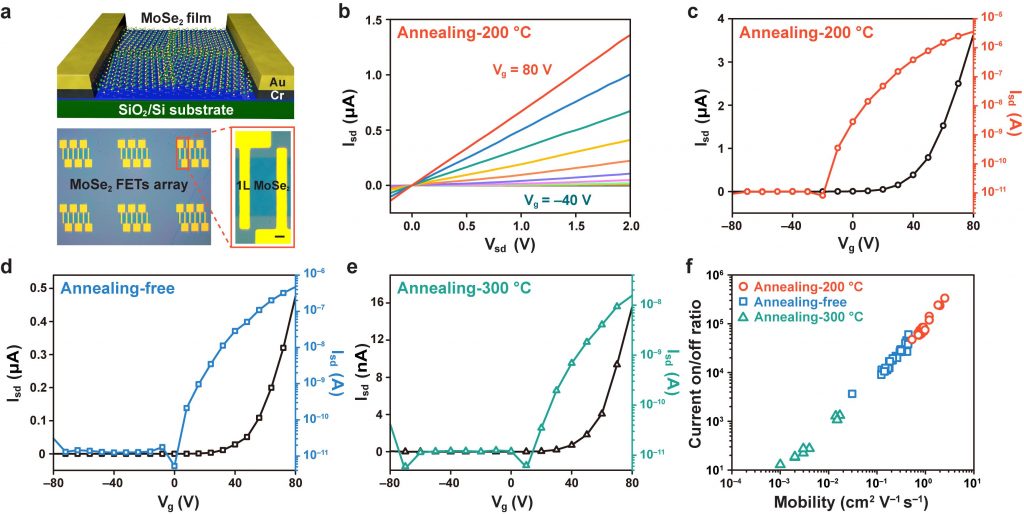
Figure 2. Electrical characteristics of the monolayer MoSe2 film. (a) Schematic of monolayer MoSe2 FET device on a SiO2/Si substrate. The inset shows an OM image of an array of MoSe2 devices with a channel length of 25 μm (scale bar: 10 μm). (b) Output characteristics of MoSe2 FET under various gate biases from Vg = −40-80 V. (c-e) Transfer characteristics of MoSe2 FET treated under different annealing conditions at Vsd = 2 V. (f) Statistical comparison plot of the field-effect mobility and current on/off ratio for the MoSe2 devices.
Researchers further synthesized various other monolayer TMD films, including molybdenum disulfide, tungsten disulfide, and tungsten diselenide, to demonstrate the broad applicability of the proposed approach. The research team also succeeded in manufacturing semiconductor devices, using the synthesized semiconductor thin films. They fabricated the MoSe2-based field effect transistors (FETs) and confirmed its superior electronic properties (i.e., Electron mobility).
The findings of this research have been published in the February 2021 issue of ACS Nano. It has been supported by the National Research Foundation of Korea (NRF) through the mid-career reesearcher program.
Journal Reference
Minseong Kim, Jihyung Seo, Jihyun Kim, et al., "High-Crystalline Monolayer Transition Metal Dichalcogenides Films for Wafer-Scale Electronics," ACS Nano, (2021).


