
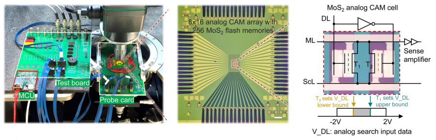
The image shows the analogue content-addressable memory (CAM) array chip built with atomically thin two-dimensional MoS2 flash memories. By using semimetal antimony (Sb) contacts, the devices achieve ultra-fast, highly energy-efficient in-memory search operations.
The explosion of artificial intelligence (AI) and the era of Big Data have exposed a critical flaw in traditional computer hardware: the slow and energy-consuming data transfer between memory and processors, commonly known as the von Neumann bottleneck. Every day, when our devices process AI queries, they must move massive amounts of data back and forth, causing severe delays and battery drain.
To address this challenge, researchers at The University of Hong Kong (HKU) have created a chip with a minimalist architecture that performs complex searches directly where the data is stored, fundamentally bypassing this bottleneck. The research team, led by Professor Can Li from the Department of Electrical and Computer Engineering of the Faculty of Engineering and the Centre for Advanced Semiconductors and Integrated Circuits (CASIC), has developed a novel analogue content-addressable memory (CAM) utilising two-dimensional (2D) MoS2 flash memories.
Content-addressable memories (CAMs) offer a promising solution by comparing input search data against all stored data simultaneously. However, traditional digital CAMs based on Static Random-Access Memory (SRAM) require up to 16 transistors (16T) per cell, resulting in bulky, power-hungry chips that can only process basic digital signals. The HKU team achieved a massive architectural leap: using MoS2, a 2D material tens of thousands of times thinner than a human hair, their analogue CAM requires only two transistors (2T) per cell. This not only shrinks the chip footprint but also allows it to directly process continuous analogue signals, which are closer to the real world, drastically increasing information density.
To make this possible, the team had to overcome the "Schottky barrier"—a wall that restricts electron flow when connecting 2D materials to circuits. The HKU team used antimony (Sb), a semimetal, as the contact electrode, effectively dismantling this barrier and creating a smooth, low-resistance pathway.
The resulting device is incredibly fast and efficient. The fabricated analogue CAM array demonstrated a high read-out current of over 60 μA/μm and an ON/OFF ratio exceeding 109. It achieved a record-breaking energy consumption of under 0.1 femtojoules (fJ) per search per cell, and a latency of just 36 picoseconds. To put this in perspective, light travels only 0.3 millimetres in one picosecond; the search is completed before light can even travel across the chip itself.
The breakthrough was the result of a highly coordinated collaborative effort. Dr Guoyun Gao, a co–first author of the paper, led the design and fabrication of the device and array, thereby achieving the observed high performance. In parallel, Mr Bo Wen conducted the array measurements, which established the linkage between the device and its search applications.
The team also demonstrated the technology's advanced potential. Through 3D heterogeneous integration, they vertically stacked N-type MoS2 and P-type WSe2 within a single CAM cell. This architecture not only halves the area required but eliminates the need for peripheral inverter circuits, further reducing power consumption.
When tasked with calculating the analogue Hamming distance for machine learning classification, the new analogue CAM performed the task approximately 108 (100 million) times faster than a standard CPU, scoring exceptionally high accuracy across multiple datasets.
"From an application perspective, search operations are incredibly valuable," explained Professor Li. "The 'attention mechanism' that serves as the foundation for Large Language Models (LLMs) is essentially a search process—retrieving information from a compressed knowledge base. We are exploring how to use this high-performance hardware to implement search mechanisms for large AI models."
The breakthrough also paves the way for ultra-compact AI chips that operate locally on edge devices. "Tasks like smartphone facial recognition could be completed instantly on the device without uploading private data to the cloud," Professor Li added. "While large-scale commercialisation still requires overcoming engineering challenges in packaging, this research has successfully proven the principle, providing a clear blueprint for next-generation, high-performance AI hardware."
The research article titled "Sb-contacted MoS2 flash memory for analogue in-memory searches" was published in Nature Nanotechnology.
Link to the paper: https://www.nature.com/articles/s41565-025-02089-7.
About Professor Can Li
Professor Can Li is an Associate Professor in the Department of Electrical and Computer Engineering of the Faculty of Engineering at HKU and serves as Associate Director of the Centre for Advanced Semiconductors and Integrated Circuits at The University of Hong Kong. He earned his BS and MS from Peking University and his PhD from the University of Massachusetts Amherst, and previously worked at Hewlett Packard Labs before joining HKU. His group develops brain-inspired, memristor- and new-material-based computing hardware to overcome the limits of von Neumann architectures and enable energy-efficient AI, with applications spanning large-scale AI, quantum-inspired optimisation, and real-time genomic analysis. This work is regularly published in venues including Nature Nanotechnology and other Nature-series journals and IEEE IEDM. He is a Clarivate Highly Cited Researcher (2025) and a recipient of the Croucher Tak Wah Mak Innovation Award and the NSFC Excellent Young Scientists Fund.


