Gary Cheng, professor in Purdue University's School of Industrial Engineering, has developed several patented laser techniques, including a nanomanufacturing platform to achieve ultrafine-scale, 3D manipulation of metals and nanomaterials. (Image provided by Gary Cheng)
Patented laser innovations have applications in consumer devices, aerospace and naval industries, plasmonics, sensing, and quantum information
WEST LAFAYETTE, Ind. – Industrial manufacturers and academic researchers can use patented, innovative laser techniques developed at Purdue University to produce high-tech materials such as semiconductor oxide thin films and metals with high performance under extreme conditions and conduct ultrafine-scale manipulation of physical properties in nanomaterials.
Gary Cheng has created innovations that improve upon traditional techniques of laser shock peening, nanowire shaping and transparent film processing. He is a professor in the School of Industrial Engineering and has a courtesy appointment in the School of Materials Engineering.
The innovations have been tested and validated, and the results have been published in peer-reviewed journals including Advanced Materials, Materials Today, Matter, Nature Communications, Science and Science Advances.
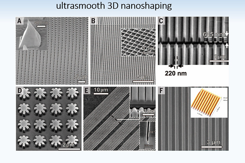
Nanoshaping platform
Cheng and his colleagues have invented a laser-based nanomanufacturing platform to achieve ultrafine-scale (down to sub-5 nanometers), 3D manipulation of metals and nanomaterials. The platform enables precise patterning, integration and strain-engineering.
It has led to applications such as opening a large band gap in graphene and fine-tuning the spacing between 2D materials and quantum dots, nanowires and nanodiamonds. There are applications in plasmonics, sensing, quantum information and nanophononics.
"Using a laser to manipulate the force and temperature on nanomaterials at an ultrafine scale creates opportunities for 3D micro/nano-component manufacturing, including patterning and integration of 0D-2D heterostructured nanomaterials," Cheng said. "This generates opportunities for developing new generations of miniature devices in fields like semiconductors, nanoelectronics and quantum technology."
Laser-assisted processing of thin films and nano-inks
Cheng's laser-based processing of thin films and nanomaterial inks addresses challenges in microstructure, defects, residual stress control and performance stability for thin film. It offers scalable manufacturing for high-performance and reliable optoelectronics and photovoltaics.
Large consumer devices like flat-panel displays, light-emitting diodes and photovoltaic cells depend on transparent conducting oxide, or TCO, films. Oxide semiconductors also have been used for thin-film transistors in next-generation devices such as high-resolution liquid crystal displays, organic light-emitting diode displays and flexible electronics.
 Purdue professor Gary Cheng and his colleagues have manufactured semiconductor oxide thin films by combining pulsed laser deposition with laser annealing to achieve better structural and optoelectronic properties than traditionally manufactured films. (Image provided by Gary Cheng)
 "The traditional material to create TCO films has been indium tin oxide," Cheng said. "Currently, semiconductor oxides such as gallium-doped zinc oxides and gallium-doped tin oxides are under research and development to replace it. Physical vapor deposition manufactures these thin films with high electron conductivity, however, their performance cannot meet the commercial criteria in performance and high-rate production."
Cheng and his colleagues have manufactured semiconductor oxide thin films by combining pulsed laser deposition with laser annealing to achieve better structural and optoelectronic properties than traditionally manufactured films. To realize large-scale thin-film device manufacturing, his team also combined roll-to-roll printing of nano-inks with laser annealing for high-quality crystalline low-defect thin film, to deposit nanolayers from nanoparticles, nanowires and 2D materials like graphene and molybdenum disulfide.
"This method achieved superior performance compared with traditional deposition techniques, especially when various materials need to be deposited sequentially, making it attractive for large-scale manufacturing," Cheng said. "There are potential applications with various nanomaterials and other deposition methods such as sol-gel printing and spray coating."
Nanostructure-integrated laser shock peening
Traditional laser shock peening, or LSP, works the surface of a metal to improve its material properties like resistance to fatigue and corrosion. The surface is confined by a glass or liquid barrier and then exposed to short laser pulses. The pulses create a shockwave that travels into the metal to deform the surface at an ultrahigh strain rate, which generates beneficial microstructure and residual stress.
Cheng said traditional LSP has drawbacks.
"Traditionally the microstructure and residual stresses are not stable after long fatigue cycles, especially under extreme conditions," Cheng said. "In addition, traditional LSP has a challenge to treat high-strength metals using water as confinement."
Cheng's innovation, called nanostructure-integrated laser shock peening, or nLSP, controls the temperature during the process to introduce nanostructures such as ultrafine and high-density nanoscale phases and dislocations. These nanostructures stabilize the beneficial microstructure and residual stress. His research has applications in the aerospace and naval industries to address the reliability of materials under extreme conditions.
"Using the method, we have shown the efficiency of nLSP on aluminum and titanium alloys with much faster processing speed and stronger shock pressure, while nanostructures can also be introduced to enhance the metals' mechanical properties and stability," he said.
Cheng has received financial support to conduct his research from the National Institute of Standards and Technology, National Research Council, National Science Foundation, Office of Naval Research and Purdue Office of Research.
Cheng disclosed these laser-related innovations to the Purdue Innovates Office of Technology Commercialization, which has applied for and received patents to protect the intellectual property. Industry partners interested in commercializing the materials for the marketplace should contact Parag Vasekar


